Renesas Electronics 5V41064NLG — Clock & Timing ICs

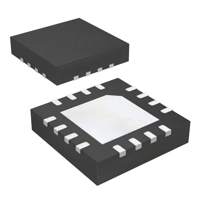
Renesas 5V41064NLG PCIe Clock Generator, 100 MHz, 16-QFN

MPN5V41064NLG
End of Life

Renesas Electronics 5V41064NLG PCI Express (PCIe) clock generator IC, PLL Yes, 100 MHz max, HCSL/LVDS output, 3.135-3.465 V, 16-VFQFN Exposed Pad, Tray.

$4.71Ref. price · indicative, final on quote
Packaging16-VFQFN Exposed Pad
StockContact for availability
Lead timeIn Stock wk
MOQ1 pcs
  • 100% new & originalTraceable channels only — no refurbs, no pulls, no remarked parts.
  • Date & lot codes on quoteStated per line before you commit; label photos on request.
  • MSL-compliant ESD packingMoisture-sealed bags with indicator cards; reels photo-verified.
  • PayPal buyer protectionPay by T/T, PayPal or Payoneer — card payments covered end to end.

Specifications

5V41064NLG Technical Specifications
ParameterValue
Mounting typeSurface Mount
Voltage3.135V ~ 3.465V
Frequency100MHz
Operating temperature0°C ~ 70°C
PLLYes
InputClock, Crystal
OutputHCSL, LVDS
PackageTray
Main purposePCI Express (PCIe)
Case16-VFQFN Exposed Pad
Number of circuits1
Ratio - Input:Output1:1
Differential - Input:OutputNo/Yes

Product details

Active PCIe reference clock generator — 100 MHz, 1:1 fanout

The 5V41064NLG is an active-production PCI Express (PCIe) clock generator from Renesas, built around a PLL that accepts a clock or crystal input and delivers a single 100 MHz differential output in HCSL or LVDS format.

3.3 V supply, commercial temperature, differential output

Operating from a 3.135 V to 3.465 V rail, the part stays within the standard 3.3 V ±5 % tolerance — the same supply that powers the PCIe root complex or switch ASIC, so no extra regulator is needed. The differential output (No/Yes input-to-output) means the input is single-ended but the output is differential HCSL or LVDS — the common-mode rejection on the PCIe receiver side rejects ground noise picked up between the clock source and the load.

16-VFQFN with exposed pad — board integration note

The supply voltage tolerance is tight enough that a 100 nF ceramic cap at each supply pin, placed within 2 mm of the pin, keeps the high-frequency noise below the PLL's jitter budget.

Frequently asked questions

What is the difference between 5V41064NLG and 5V41064NLGI?

Both share the same PLL, 100 MHz output, HCSL/LVDS signalling, and 16-VFQFN package — the only difference is the operating temperature range.