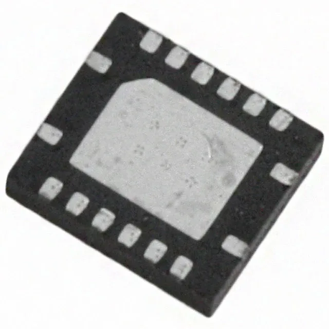
Renesas Electronics 5V2305NRGI8 — Clock & Timing ICs

Renesas 5V2305NRGI8 Fanout Buffer, 200 MHz, 1:5, 16-VFQFPN

MPN5V2305NRGI8
End of Life

Renesas 5V2305NRGI8 Fanout Buffer (Distribution), 1:5 LVCMOS/LVTTL input to LVCMOS output, 200 MHz max, 2.3 V to 3.6 V supply, -40°C to 85°C, 16-VFQFPN (3.5x4 mm) exposed pad, Surface Mount.

$3.83Ref. price · indicative, final on quote
Packaging16-VFQFN Exposed Pad
StockContact for availability
MOQ1 pcs
  • 100% new & originalTraceable channels only — no refurbs, no pulls, no remarked parts.
  • Date & lot codes on quoteStated per line before you commit; label photos on request.
  • MSL-compliant ESD packingMoisture-sealed bags with indicator cards; reels photo-verified.
  • PayPal buyer protectionPay by T/T, PayPal or Payoneer — card payments covered end to end.

Specifications

5V2305NRGI8 Technical Specifications
ParameterValue
TypeFanout Buffer (Distribution)
Mounting typeSurface Mount
Voltage2.3V ~ 3.6V
Frequency200 MHz
Operating temperature-40°C ~ 85°C
InputLVCMOS, LVTTL
OutputLVCMOS
PackageTape & Reel (TR); Cut Tape (CT)
Case16-VFQFN Exposed Pad
Number of circuits1
Ratio - Input:Output1:5
Differential - Input:OutputNo/No

Product details

Industrial temperature and active lifecycle

Rated -40°C to 85°C, this buffer is suited for industrial environments — factory automation, outdoor telecom cabinets, motor drives, and base-station line cards where the ambient swings but stays below the 85°C ceiling.

Non-differential input — what that means for your clock tree

Both the input and output are single-ended (LVCMOS/LVTTL in, LVCMOS out); there is no differential pair like LVPECL or LVDS. That simplifies the layout — no termination resistors or bias networks — but it also means the buffer does not reject common-mode noise on the input. Keep the trace short and route it away from switching power rails to avoid coupling into the clock path.

Frequently asked questions

What is the maximum frequency supported by 5V2305NRGI8?

200 MHz. That is the ceiling for the LVCMOS output; the input side is rated for the same frequency. Good for distributing a 100 MHz or 125 MHz reference, but not for gigabit-rate clocks.