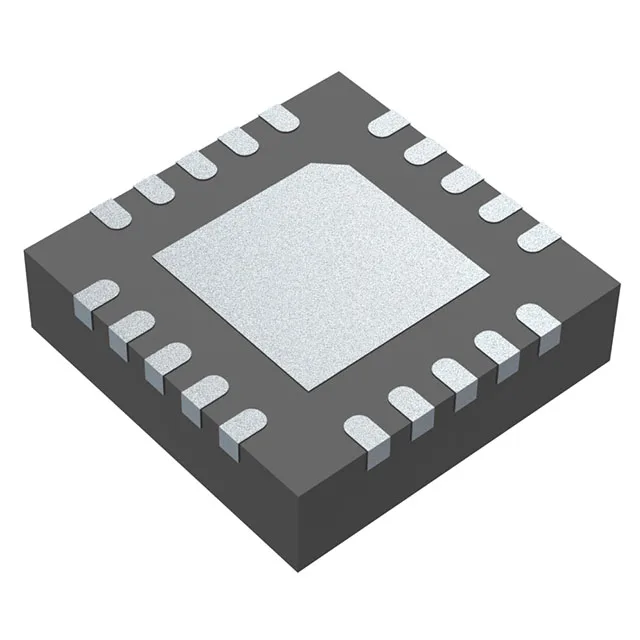
Renesas Electronics 5PB1206NDGK — Clock & Timing ICs

5PB1206NDGK Fanout Buffer, 1:6 LVCMOS, 200 MHz, 20-QFN

MPN5PB1206NDGK
End of Life

Renesas 5PB1206NDGK Fanout Buffer (Distribution), 1:6 LVCMOS input/output, 200 MHz max frequency, 1.71V to 3.465V supply, -40°C to 105°C, 20-VFQFN Exposed Pad (3x3 mm).

$3.19Ref. price · indicative, final on quote
Packaging20-VFQFN Exposed Pad
StockContact for availability
MOQ1 pcs
  • 100% new & originalTraceable channels only — no refurbs, no pulls, no remarked parts.
  • Date & lot codes on quoteStated per line before you commit; label photos on request.
  • MSL-compliant ESD packingMoisture-sealed bags with indicator cards; reels photo-verified.
  • PayPal buyer protectionPay by T/T, PayPal or Payoneer — card payments covered end to end.

Specifications

5PB1206NDGK Technical Specifications
ParameterValue
TypeFanout Buffer (Distribution)
Mounting typeSurface Mount
Voltage1.71V ~ 3.465V
Frequency200 MHz
Operating temperature-40°C ~ 105°C (TA)
InputLVCMOS
OutputLVCMOS
PackageTray
Case20-VFQFN Exposed Pad
Number of circuits1
Ratio - Input:Output1:6
Differential - Input:OutputNo/No

Product details

What this 1:6 LVCMOS fanout buffer does on your clock tree

The Renesas 5PB1206NDGK is a single-circuit fanout buffer that takes one LVCMOS clock input and distributes it to six LVCMOS outputs. It's a non-differential, non-inverting buffer — what goes in as a clean LVCMOS edge comes out as six copies, no level translation, no signal inversion. The part handles clock rates up to 200 MHz, which covers most microcontroller, FPGA, and Ethernet PHY reference clock distribution needs in systems that don't require differential signalling like LVPECL or LVDS.

Temperature grade and operating environment

Rated for -40°C to 105°C ambient, this buffer fits industrial control, outdoor telecom, and automotive cabin environments.

Lifecycle and sourcing reality

No end-of-life notice, no last-time-buy window to track.

Frequently asked questions

Is 5PB1206NDGK obsolete or active?

Active. Renesas lists the 5PB1206NDGK as current production with no end-of-life notice. It is also ROHS3 compliant, so no RoHS transition issues for new builds.

What is the maximum frequency of 5PB1206NDGK?

200 MHz is the maximum frequency. That covers most common clock distribution needs — 100 MHz Ethernet reference clocks, 50 MHz MCU oscillators, 25 MHz PHY crystals — but not gigabit SerDes or RF clocking above 200 MHz.

Are there equivalent parts to 5PB1206NDGK?

The closest functional peer is the 5PB1104CMGK/W, which is the same Renesas family with a 1:4 fanout instead of 1:6. It shares the same LVCMOS levels, 200 MHz max frequency, and 1.71 V supply minimum, but in a different package option (Tape & Reel). If you need exactly six outputs, the 5PB1206NDGK is the one; if four outputs suffice, the 5PB1104CMGK/W is a drop-in consideration for BOM consolidation.

What is a fanout clock buffer?

A fanout clock buffer takes one clock input signal and produces multiple identical copies of that signal, each with enough drive strength to travel across a PCB trace to a different load. The 5PB1206NDGK specifically takes one LVCMOS input and gives you six LVCMOS outputs, all phase-aligned to the input.

How does a 1:6 clock buffer work?

The 1:6 ratio means one input pin feeds six output pins through internal buffer stages. Each output is a replica of the input waveform, but with higher drive capability so it can charge the capacitance of a long trace and the input pin of a downstream device. The non-differential design means no signal conversion — LVCMOS in, LVCMOS out.