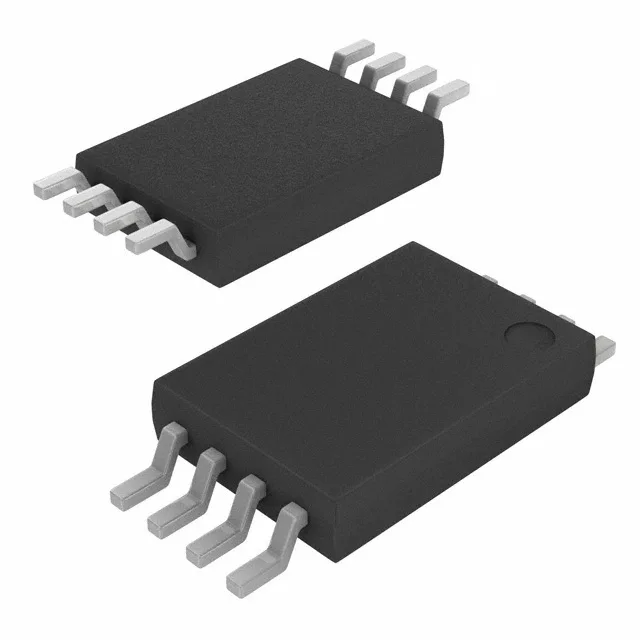
Renesas Electronics 5PB1104CMGK/W — Microcontrollers & Processors (MCU / MPU / DSP)

Renesas 5PB1104CMGK/W Clock Buffer, 200 MHz, 1:4, LVCMOS

MPN5PB1104CMGK/W
End of Life

Renesas Electronics 5PB1104CMGK/W Clock Buffer, LVCMOS input/output, 200 MHz max, 1:4 fanout, 8-UFDFN package, surface mount, -40°C to 105°C.

$1.9Ref. price · indicative, final on quote
Packaging8-UFDFN
RoHSROHS3 Compliant
Independent supplier — new & surplus stockAuthenticity-screened · ESD-safe packingListing updated Aug 2026

Specifications

5PB1104CMGK/W specifications
ParameterValue
TypeClock Buffer
MountingSurface Mount
Supply voltage1.71V ~ 1.89V, 2.375V ~ 2.625V, 3.135V ~ 3.465V
Frequency - max200 MHz
Operating temperature-40°C ~ 105°C (TA)
InputLVCMOS
OutputLVCMOS
PackageTape & Reel (TR); Cut Tape (CT)
Case8-UFDFN
Number of circuits1
Ratio - Input:Output1:4
Differential - Input:OutputNo/No

Product details

Active production, 1:4 fanout, three supply ranges

The 5PB1104CMGK/W is a 1:4 fanout clock buffer from Renesas, accepting a single LVCMOS input and distributing it to four LVCMOS outputs at up to 200 MHz.

The differential input/output flag is No/No, meaning this is a single-ended buffer — no CML or LVPECL termination network needed on the board.

Frequently asked questions

What is the closest functional alternative to 5PB1104CMGK/W?

The 5PB1104PGGK is the same die in the same 8-pin package, with the same 1:4 fanout, 200 MHz limit, and LVCMOS I/O — the only difference is the shipping media (tube vs tape/reel). No board change is needed to swap between them.

What compliance documentation does Renesas provide for 5PB1104CMGK/W?

Renesas certifies ROHS3 compliance for this part number. No UL, IEC, or REACH documentation is listed in the product record.