What this 1:4 fanout buffer does on your clock tree
The IDT 524MILFT is a single-circuit fanout buffer from the ClockBlocks™ family that takes one clock input and distributes it to four CMOS outputs. It handles clock frequencies up to 200 MHz, making it a straightforward choice for splitting a reference clock to multiple loads — FPGA banks, multiple ADCs, or a set of SerDes transceivers — without adding differential routing complexity. The non-differential input and output (No/No) mean you feed it a single-ended clock and get back four single-ended CMOS copies.
Supply range and temperature — where it fits on the board
The 2.375V to 5.25V supply range covers 2.5V, 3.3V, and 5V logic rails without a separate regulator. That wide compliance simplifies BOM consolidation when the board already runs mixed-voltage domains.
8-SOIC package — rework-friendly and board-fit
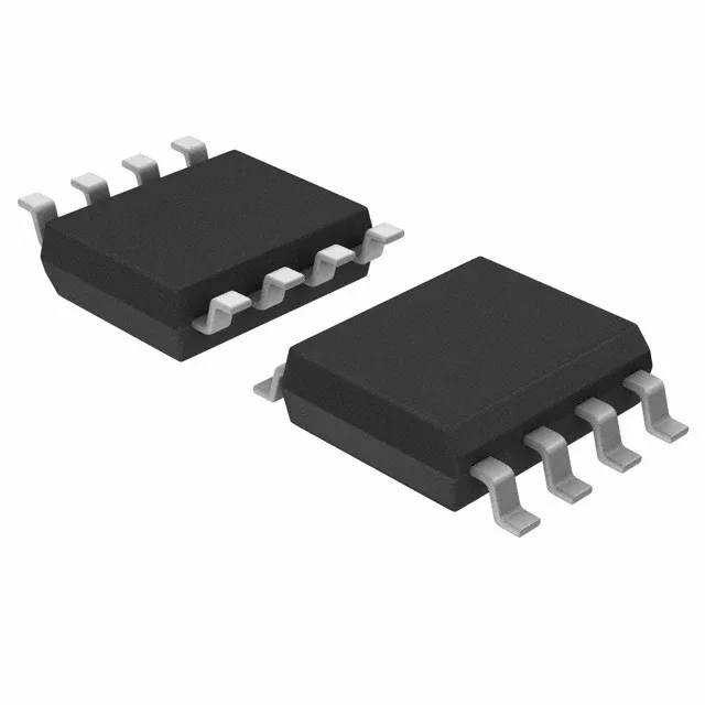
The 8-SOIC package (0.154" body width, 3.90 mm) is a standard footprint that hand-rework handles easily. No thermal pad underneath, so no via-stitch requirement — just a clean, two-layer-routable layout. Will it survive the hot air? Yes, with a standard 260°C peak profile and no moisture sensitivity surprises (MSL 1 typical for this package class).