Clock distribution for synchronous logic
The 23S09T-1DCG is a zero-delay buffer that generates nine synchronized copies of a single LVTTL reference clock, with the PLL aligning the output edges to the input to within the device's static phase offset. Maximum operating frequency of 133 MHz covers common bus clocks for DDR, PCI, and Ethernet MAC interfaces, though the non-differential I/O means it is suited for single-ended clock trees rather than differential pairs like LVDS or HCSL. The PLL bypass mode lets the input clock pass directly to the outputs without phase alignment — useful for test, low-frequency operation where PLL lock time is unacceptable, or when the reference clock is already jitter-compliant and only fanout is needed.
Supply rail and temperature grade
The 1:9 fanout ratio with no internal divider or multiplier means the output frequency equals the input frequency — the part does not synthesize higher or lower clocks, it only buffers and phase-aligns.
Package and board integration
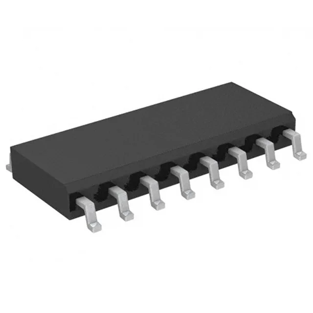
Housed in a 16-SOIC package with 3.90 mm body width, the footprint matches industry-standard SOIC-16 land patterns. Surface-mount assembly with a 1.27 mm pitch is straightforward for standard reflow profiles and does not require via-in-pad or microvia fanout.
No official second-source or pin-compatible cross-reference is recorded in the manufacturer's documentation. The closest parametric peer is the 23S05-1DCG, which offers a 1:5 fanout ratio instead of 1:9 — the package and supply voltage differ, so a board spin would be required for substitution.