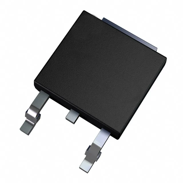
FDD2570
onsemi
-55°C ~ 150°C (TJ)Tape & Reel (TR)PowerTrench®
Ref. price$1.4600
Lead time on requestGet quote
13 variants · onsemi
The onsemi FDD2 Series series groups 13 related part numbers, each listed with full specifications, a datasheet where available, and an RFQ option. The listed variants share a common FET feature of -, FET type of N-Channel and mounting of Surface Mount. Variants differ by case, current - continuous drain (Id) @ 25°C and drain to source voltage, so you can match the exact case your application requires using the selection guide below.
| Parameter | FDD2570 | FDD26AN06A0 |
|---|---|---|
| Case | TO-252-3, DPak (2 Leads + Tab), SC-63 | TO-252-3, DPAK (2 Leads + Tab), SC-63 |
| Current - continuous drain (Id) @ 25°C | 4.7A (Ta) | 7A (Ta), 36A (Tc) |
| Drain to source voltage | 150 V | 60 V |
| Drive voltage (Max rds on, min rds on) | 6V, 10V | 10V |
| Gate charge (Qg) (Max) @ vgs | 62 nC @ 10 V | 17 nC @ 10 V |
| Input capacitance (Ciss) (Max) @ vds | 1907 pF @ 75 V | 800 pF @ 25 V |
| Operating temperature | -55°C ~ 150°C (TJ) | -55°C ~ 175°C (TJ) |
| Power dissipation | 3.2W (Ta), 70W (Tc) | 75W (Tc) |
Request a quote on any onsemi FDD2 Series part number and we confirm price, availability and lead time per line — including end-of-life and allocation-constrained variants.
onsemi
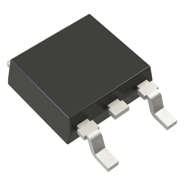
onsemi