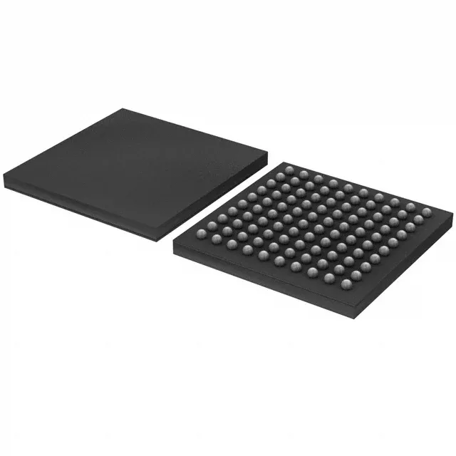
NXP USA Inc. LPC43S30FET100E — Microcontrollers & Processors (MCU / MPU / DSP)

NXP LPC43S30FET100E Dual-Core MCU, 204MHz, 264KB SRAM, 100-TFBGA

MPNLPC43S30FET100E
Active

NXP LPC43xx series, LPC43S30FET100E, dual-core 32-bit ARM Cortex-M4/M0 MCU, 204MHz, 264K x 8 SRAM, ROMless, 49 I/O, CANbus, Ethernet, USB OTG, 100-TFBGA 9x9mm, 2.2–3.6V, -40°C to 85°C.

$12.5900Ref. price · indicative, final on quote
Independent supplier — new & surplus stockAuthenticity-screened · ESD-safe packingListing updated Jul 2026

Specifications

LPC43S30FET100E specifications
ParameterValue
SeriesLPC43xx
MountingSurface Mount
Oscillator typeInternal
Program memory typeROMless
Voltage - supply (Vcc (Vdd))2.2V ~ 3.6V
Operating temperature-40°C ~ 85°C (TA)
Speed204MHz
PackageTray
RAM size264K x 8
Core size32-Bit Dual-Core
PeripheralsBrown-out Detect/Reset, DMA, I²S, POR, WDT
ConnectivityCANbus, EBI/EMI, Ethernet, I²C, IrDA, Microwire, SD, SPI, SSI, SSP, UART/USART, USB, USB OTG
Number of i (O)49
Core processorARM® Cortex®-M4/M0
Case100-TFBGA
Data convertersA/D 4x10b; D/A 1x10b

Product details

The NXP LPC43S30FET100E pairs a Cortex-M4 application core with a Cortex-M0 coprocessor, both clocked at 204 MHz. The M4 handles the main control loop and protocol stacks; the M0 offloads real-time I/O, sensor polling, or bit-banged serial interfaces without jitter on the M4 side. For a gateway or motor-drive controller that must run an Ethernet stack and a CANopen fieldbus simultaneously, that split saves a second MCU.

ROMless program memory — plan for external Flash

This part has no internal Flash — program memory is ROMless. Boot code must reside in external SPI NOR or parallel NAND Flash, accessed through the EBI/EMI or SSP interface.

Connectivity set — CANbus, Ethernet, USB OTG

The peripheral list covers CANbus, Ethernet, USB OTG, multiple I²C/SPI/UART, plus an EBI/EMI for parallel memory or FPGA glue. That makes the LPC43S30FET100E a natural fit for an industrial IoT gateway that bridges a CANopen machine network to an Ethernet-based SCADA system, or for a motor drive that logs data over USB. The 49 I/O count is tight for a 100-ball BGA — expect to multiplex address/data lines on the EBI if you need both external memory and a parallel display.

The 100-TFBGA (9×9 mm) package keeps board area small.

Frequently asked questions

What is the closest pin-compatible alternative to the LPC43S30FET100E?

The LPC43S30FET100E is a ROMless variant in the LPC43xx family. Pin-compatible alternatives exist within the same family (e.g., LPC43S50FET100 with larger SRAM or LPC43S67FET100 with on-chip Flash), but the exact memory and peripheral mix should be verified against the target application.

What is the listed speed of the LPC43S30FET100E?

The LPC43S30FET100E runs both Cortex-M4 and Cortex-M0 cores at 204 MHz.

What compliance documentation does NXP provide for the LPC43S30FET100E?

NXP provides RoHS and REACH compliance declarations for the LPC43S30FET100E; UL and IEC certifications are not listed in the standard documentation set for this part.