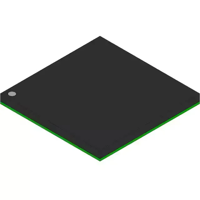
NXP USA Inc. LPC4353JET256551 — Microcontrollers & Processors (MCU / MPU / DSP)

NXP LPC4353JET256551 32-bit Dual-Core MCU, 204MHz, 512KB Flash

MPNLPC4353JET256551
Active

NXP LPC43xx series, 32-bit dual-core ARM Cortex-M4/M0 MCU, 204MHz, 512KB Flash, 136KB SRAM, 164 I/O, Motor Control PWM, Ethernet, USB OTG, CAN, -40 to 105°C, 2.2–3.6V, 256-LBGA package, bulk.

Independent supplier — new & surplus stockAuthenticity-screened · ESD-safe packingListing updated Jul 2026

Specifications

LPC4353JET256551 specifications
ParameterValue
SeriesLPC43xx
MountingSurface Mount
Oscillator typeInternal
Program memory typeFLASH
Voltage - supply (Vcc (Vdd))2.2V ~ 3.6V
Operating temperature-40°C~105°C(TA)
Speed204MHz
PackageBulk
RAM size136K x 8
Core size32-Bit Dual-Core
EEPROM size16K x 8
PeripheralsBrown-out Detect/Reset, DMA, I²S, LCD, Motor Control PWM, POR, PWM, WDT
ConnectivityCANbus, EBI/EMI, Ethernet, I²C, IrDA, Microwire, QEI, SD, SPI, SSI, SSP, UART/USART, USB, USB OTG
Number of i (O)164
Core processorARM® Cortex®-M4/M0
Case256-LBGA
Data convertersA/D 8x10b; D/A 1x10b
Program memory size512KB (512K x 8)

Product details

Dual-core split for motion and HMI

The NXP LPC4353JET256551 runs a 32-bit dual-core ARM Cortex-M4 at 204 MHz paired with a Cortex-M0, giving you a dedicated real-time control core and a separate housekeeping core on one die. The M4 handles the motor-control PWM loops and Ethernet stack; the M0 takes care of CAN message handling, I²C sensor polling, and the LCD refresh. That split keeps the control loop jitter off the fieldbus traffic. Program memory is 512 KB of on-chip Flash, backed by 136 KB SRAM and 16 KB EEPROM — enough for a moderate motor-drive application with a local HMI screen. The 164 I/O lines break out to a 256-LBGA package (17x17 mm), so board layout needs a four-layer stackup minimum to route the EBI/EMI and Ethernet traces cleanly.

What the 204 MHz dual-core means for your BOM

Compared to a single-core Cortex-M4 at the same clock, this part lets you run the motor-control ISR on the M4 without the M0's CAN interrupt jitter affecting it. That means you can skip an external CAN controller or a second MCU for the fieldbus gateway — one chip does both. The trade-off is the 256-ball BGA footprint: if your assembly house isn't set up for fine-pitch BGA rework, factor in a stencil and X-ray inspection step.

Peripheral set and deployment context

Frequently asked questions

What is the closest pin-compatible alternative to LPC4353JET256551?

No pin-compatible second source is listed in the official documentation. The LPC43xx family includes density variants (e.g., LPC4357 with 1 MB Flash) that share the same 256-LBGA footprint, but verify the memory map and peripheral set against your firmware before swapping.

What compliance documentation does NXP provide for LPC4353JET256551?

NXP provides RoHS and REACH compliance declarations for this part. The bulk package (non-tape-and-reel) may affect the declaration format — request the specific compliance certificate at quote time.