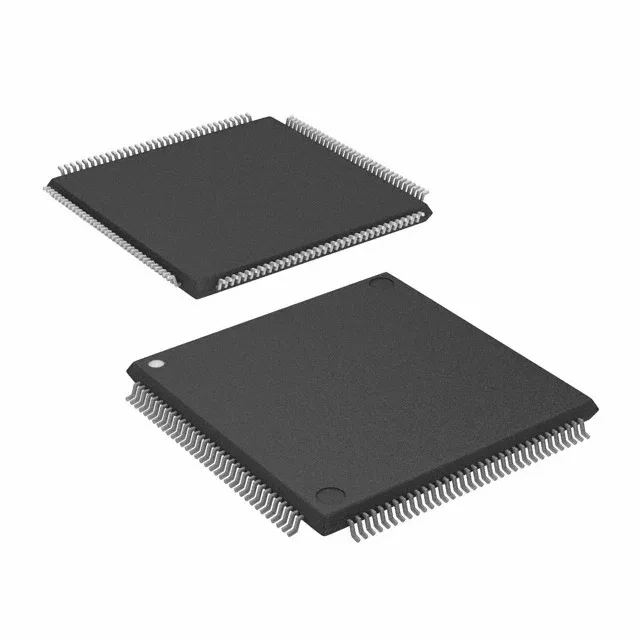
Dual-core architecture — asymmetric workload split
The LPC4333JBD144E pairs an ARM Cortex-M4 running at 204 MHz with a Cortex-M0 coprocessor. The M4 handles the DSP-heavy loops — motor-control FOC, audio processing, or protocol stacks — while the M0 offloads real-time housekeeping like GPIO polling, UART framing, or wake-up logic. That split frees the M4 from interrupt overhead and keeps deterministic timing on the control loop.
Memory map and on-chip storage
512 KB of Flash (512K x 8) holds the application image; 136K x 8 of SRAM provides working space for stacks and data buffers. There is also 16K x 8 of EEPROM for calibration constants or boot parameters that survive a full erase cycle. For a dual-core part, the SRAM is sized to keep both cores' local data in on-chip memory without thrashing an external bus.
The EBI/EMI bus extends to external memory or FPGA-style peripherals. Motor-control PWM and a quadrature encoder interface are built in — no external timer glue needed for a servo drive.
NXP lists this part as Active — no last-time-buy or phase-out notice.