204 MHz — core speed and bus margin
The LPC4327JET100E: The 204 MHz clock drives the Cortex-M4 FPU and the M0 co-processor. For a BOM that needs deterministic interrupt latency on the M4 while the M0 handles peripheral I/O, this split avoids a second MCU.
Memory sizing and field updates
1 MB of Flash (1M x 8) leaves room for a dual-bank firmware update scheme — one bank active, one staged. The 136 KB SRAM supports moderate-size frame buffers or a real-time OS heap. The 16 KB EEPROM block holds calibration constants or configuration that survives a reprogram cycle, which avoids an external serial EEPROM on the board.
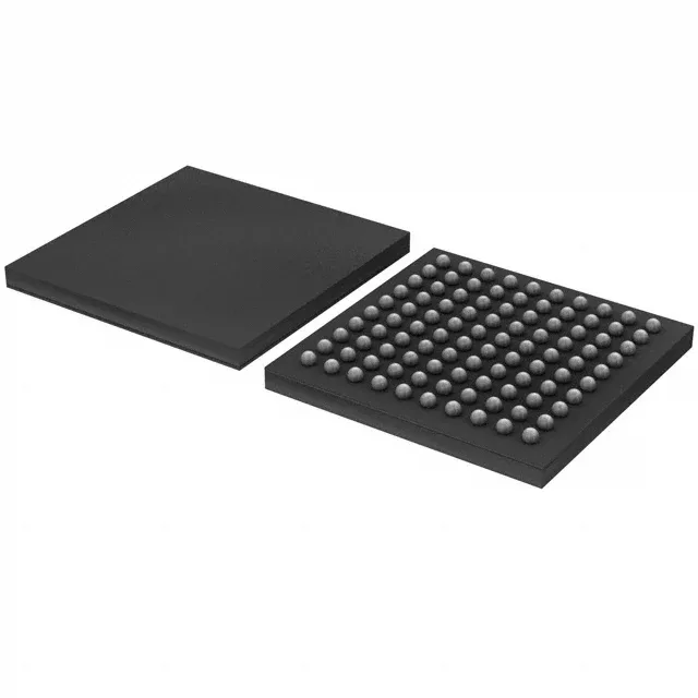
The 100-TFBGA package (9x9 mm) is a fine-pitch BGA; board assembly requires a solder-paste stencil and reflow profile matched to the package, but the footprint saves board area versus a larger QFP.