On-chip connectivity includes CANbus, USB OTG, multiple SPI/I²C/UART interfaces, and an external bus interface (EBI/EMI) for expanding memory or connecting FPGAs. The 49 GPIOs are enough for a mid-complexity control board with a local display, keypad, and a handful of sensors. The internal oscillator keeps the BOM lean for applications that do not require a precision external clock source. Data converters: a 4-channel 10-bit ADC and a single 10-bit DAC.
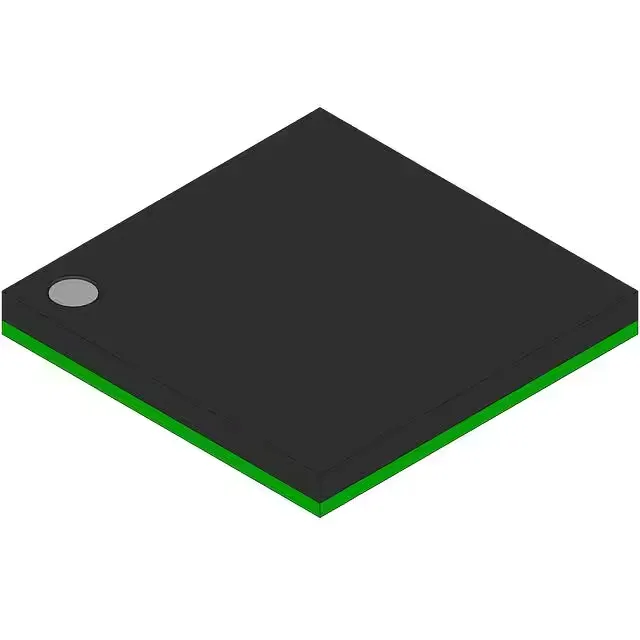
NXP LPC4325JET100551 MCU, 32-Bit Dual-Core Cortex-M4/M0, 204MHz
MPNLPC4325JET100551
Active
NXP LPC43xx series dual-core ARM Cortex-M4/M0 microcontroller, 204MHz, 768KB Flash, 136KB SRAM, 16KB EEPROM, 49 GPIO, USB OTG, CANbus, 2.2–3.6V, -40°C to 105°C, 100-TFBGA (9x9 mm).
Independent supplier — new & surplus stockAuthenticity-screened · ESD-safe packingListing updated Jul 2026
Specifications
| Parameter | Value |
|---|---|
| Series | LPC43xx |
| Mounting | Surface Mount |
| Oscillator type | Internal |
| Program memory type | FLASH |
| Voltage - supply (Vcc (Vdd)) | 2.2V ~ 3.6V |
| Operating temperature | -40°C~105°C(TA) |
| Speed | 204MHz |
| Package | Bulk |
| RAM size | 136K x 8 |
| Core size | 32-Bit Dual-Core |
| EEPROM size | 16K x 8 |
| Peripherals | Brown-out Detect/Reset, DMA, I²S, POR, WDT |
| Connectivity | CANbus, EBI/EMI, I²C, IrDA, Microwire, SD, SPI, SSI, SSP, UART/USART, USB, USB OTG |
| Number of i (O) | 49 |
| Core processor | ARM® Cortex®-M4/M0 |
| Case | 100-TFBGA |
| Data converters | A/D 4x10b; D/A 1x10b |
| Program memory size | 768KB (768K x 8) |
Product details
Frequently asked questions
What is LPC4325JET100551's listed speed?
The core runs at 204 MHz, shared between the Cortex-M4 and Cortex-M0. That clock rate gives the M4 enough headroom for DSP loops and protocol processing while the M0 handles time-critical I/O or safety tasks.
What compliance documentation does NXP provide for LPC4325JET100551?
NXP provides RoHS and REACH compliance declarations for this part. The 100-TFBGA package is lead-free and meets the current EU directive requirements. UL or IEC certification is not listed in the standard documentation set.