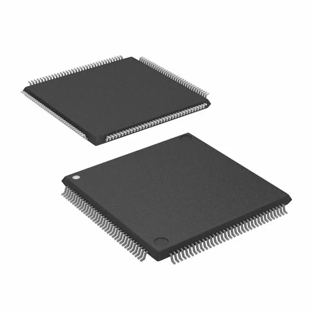
The NXP LPC4317JBD144E pairs an ARM Cortex-M4 for application processing with a Cortex-M0 for real-time control or I/O offload, both clocked at 204 MHz. This asymmetric architecture lets a motor-drive design run the field-oriented control loop on the M0 while the M4 handles HMI and communications — no separate co-processor needed. With 1 MB Flash and 136 KB RAM, this part fits firmware images that include a real-time OS, TCP/IP stack, and a modest GUI frame buffer. The 136 KB SRAM is sized for double-buffered data from the 8-channel 10-bit ADC or the SDIO interface.
The peripheral list includes CANbus, multiple SPI/I²C/UART, an external memory interface (EBI/EMI), and motor-control PWM — covering the common I/O mix for industrial drives and instrumentation.
Package and integration note
Housed in a 144-LQFP (20×20 mm) surface-mount package, this MCU occupies a standard footprint for mid-density LQFP designs. The 83 GPIOs route to the peripheral multiplexer — verify pin allocation against the datasheet's alternate-function map early in layout to avoid signal conflicts with the EBI/EMI and CANbus interfaces.