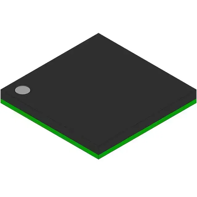
The NXP LPC4310FET100 is a 32-bit dual-core MCU built around an ARM Cortex-M4 and a Cortex-M0, clocked at 204 MHz. The M4 handles DSP and control loops; the M0 offloads I/O, protocol handling, or housekeeping tasks. With 168K x 8 SRAM and no on-chip Flash (ROMless), firmware executes from external memory via the EBI/EMI interface. This architecture suits systems that already carry external Flash or SDRAM — industrial controllers, motor drives, or communications gateways where the memory is shared across the board.
ROMless — no internal Flash, plan the external memory
The ROMless program memory type means this MCU has no internal Flash for code storage. Firmware must be fetched from external memory via the EBI/EMI interface.
Connectivity and peripherals for industrial control
On-chip connectivity includes CANbus, I²C, SPI, SSI, SSP, UART/USART, IrDA, Microwire, SD, and the EBI/EMI bus for external memory or FPGA bridging. Peripherals cover DMA, PWM, watchdog, brown-out detect, POR, and I²S for audio. The 49 I/O lines are available on the 100-TFBGA package (9x9 mm ball grid array). Supply range is 2.2 V to 3.6 V, with an internal oscillator and an operating temperature range of -40 to 85°C — suited for industrial and outdoor equipment.