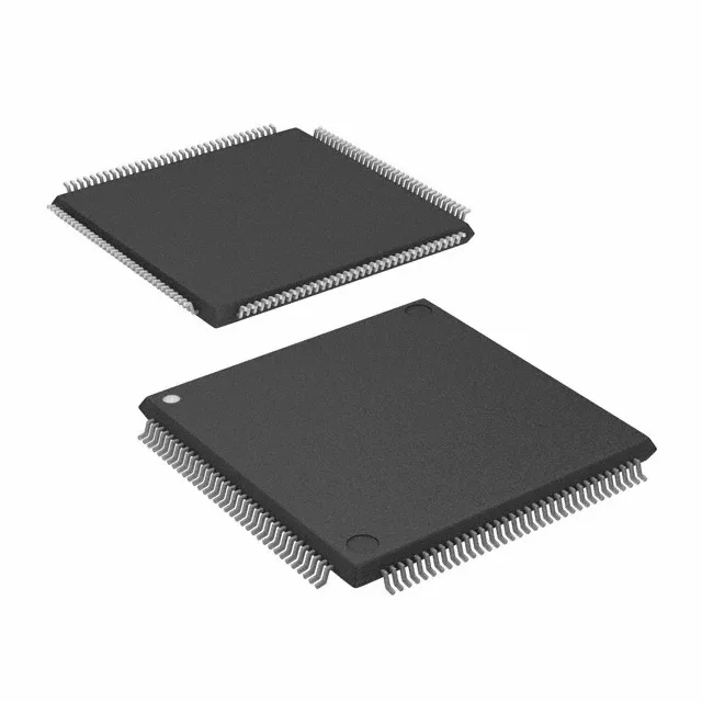
NXP USA Inc. LPC4088FBD144,551 — Microcontrollers & Processors (MCU / MPU / DSP)

NXP LPC4088FBD144,551 ARM Cortex-M4 MCU, 120MHz

MPNLPC4088FBD144,551
Active

NXP LPC40xx series 32-bit ARM Cortex-M4 MCU, LPC4088FBD144,551, 120 MHz core, 512 KB Flash, 96 KB RAM, 144-LQFP, -40 to 85 °C.

$17.9800Ref. price · indicative, final on quote
Independent supplier — new & surplus stockAuthenticity-screened · ESD-safe packingListing updated Jul 2026

Specifications

LPC4088FBD144,551 specifications
ParameterValue
SeriesLPC40xx
MountingSurface Mount
Oscillator typeInternal
Program memory typeFLASH
Voltage - supply (Vcc (Vdd))2.4V ~ 3.6V
Operating temperature-40°C ~ 85°C (TA)
Speed120MHz
PackageTray
RAM size96K x 8
Core size32-Bit Single-Core
EEPROM size4032 x 8
PeripheralsBrown-out Detect/Reset, DMA, I²S, LCD, POR, PWM, WDT
ConnectivityCANbus, EBI/EMI, Ethernet, I²C, IrDA, Microwire, QEI, SD, SPI, SSI, SSP, UART/USART, USB, USB OTG
Core processorARM® Cortex®-M4
Case144-LQFP
Data convertersA/D 8x12b; D/A 1x10b
Program memory size512KB (512K x 8)

Product details

32-bit ARM Cortex-M4 microcontroller, 120 MHz core, 512 KB Flash, 96 KB SRAM. LPC40xx series, 144-LQFP package, -40 to 85 °C operating temperature.

120 MHz Cortex-M4 — what it means for throughput

FPU handles single-precision floating-point in hardware.

Memory sizing and field-update reality

512 KB of Flash is the program store; the 96 KB SRAM partitions into a main SRAM block and a separate USB-dedicated buffer. For a typical application — say, an Ethernet-connected sensor gateway with a web server and a 320x240 LCD — the Flash holds the firmware plus a small file system, and the SRAM leaves about 40 KB free for heap and stack after the TCP/IP stack and RTOS kernel are loaded. The 4032 x 8 bytes of EEPROM emulation (simulated in Flash) handles calibration constants and network configuration that survive a power cycle. Field firmware updates are feasible via the USB OTG or Ethernet bootloader, but the 512 KB size means the update image must be compressed or streamed — there is no room for a full dual-bank swap.

Frequently asked questions

What is the maximum operating frequency of LPC4088FBD144?

The core runs at 120 MHz, which is the maximum clock for this ARM Cortex-M4 implementation in the LPC40xx series.

What is the difference between LPC4088FBD144 and LPC4088FET144?

The FBD144 suffix denotes a 144-LQFP package (20x20 mm, 0.5 mm pitch), while the FET144 suffix is a 144-BGA package. The die and core logic are identical, but the BGA variant requires a different PCB footprint and assembly process — they are not pin-compatible.

What is a direct replacement for LPC4088FBD144,551?

There is no pin-compatible direct replacement from NXP that uses the same 144-LQFP footprint. The LPC4088FET144 (BGA) shares the same die but requires a board layout change. For a like-for-like swap, order the same LPC4088FBD144,551.