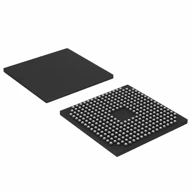
NXP USA Inc. LPC3240FET296/01551 — Microcontrollers & Processors (MCU / MPU / DSP)

NXP LPC3240FET296/01551 ARM926EJ-S MCU, 266MHz, 256KB SRAM, 296-TFBGA

MPNLPC3240FET296/01551
Active

NXP LPC3200 series ARM926EJ-S MCU, LPC3240FET296/01551, 16/32-Bit core at 266MHz, 256K x 8 SRAM, ROMless, 51 I/O, Ethernet, USB OTG, SPI/SSP/I²C, 3×10b ADC, Motor PWM, -40°C~85°C, 0.9V~3.6V, 296-TFBGA (15×15mm), Bulk, Active.

StockContact for availability
MOQ1 pcs
  • 100% new & originalTraceable channels only — no refurbs, no pulls, no remarked parts.
  • Date & lot codes on quoteStated per line before you commit; label photos on request.
  • MSL-compliant ESD packingMoisture-sealed bags with indicator cards; reels photo-verified.
  • PayPal buyer protectionPay by T/T, PayPal or Payoneer — card payments covered end to end.

Specifications

LPC3240FET296/01551 Technical Specifications
ParameterValue
SeriesLPC3200
Mounting typeSurface Mount
Oscillator typeInternal
Program memory typeROMless
Voltage - supply (Vcc (Vdd))0.9V ~ 3.6V
Operating temperature-40°C~85°C(TA)
Speed266MHz
PackageBulk
RAM size256K x 8
Core size16/32-Bit
PeripheralsDMA, I²S, Motor Control PWM, PWM, WDT
ConnectivityEBI/EMI, Ethernet, I²C, IrDA, Microwire, SPI, SSI, SSP, UART/USART, USB OTG
Number of i (O)51
Core processorARM926EJ-S
Case296-TFBGA
Data convertersA/D 3x10b

Product details

266 MHz ARM926EJ-S — what the clock buys you

The LPC3240FET296/01551 runs an ARM926EJ-S core at 266 MHz. That clock rate places it in the mid-range of the LPC3200 family — enough throughput for a real-time Ethernet stack with headroom for a control loop, but not the top-bin part if you need multiple protocol stacks or heavy DSP work. The 16/32-Bit core size means legacy 16-bit code lifts cleanly, but the compiler targets ARM mode for performance. At 266 MHz, expect bus timing to be the constraint on external memory access, not the core itself.

ROMless with 256 KB SRAM — plan for external code storage

This part has no internal Flash or ROM — program memory type is ROMless. The 256K x 8 SRAM is for data, not code. You must boot from external NOR Flash, NAND, or SRAM via the EBI/EMI interface. That means a companion memory chip on the BOM and careful PCB layout for the parallel bus. The 296-TFBGA (15x15 mm) package gives enough ball count for a wide external bus plus the peripheral I/O. The 0.9 V to 3.6 V supply range covers core and I/O voltages; the external memory will dictate the actual rail.

Peripheral set for industrial and motor control

The connectivity list is broad: Ethernet MAC, USB OTG, multiple SPI/SSP, I²C, UART/USART, plus IrDA and Microwire. The Motor Control PWM and general-purpose PWM, along with the DMA controller and the 3-channel 10-bit ADC, make this a natural fit for a servo drive or inverter control board that also needs an Ethernet fieldbus interface. The 51 general-purpose I/O are enough for a modest HMI or I/O bank, but not for a high-density PLC backplane. Operating temperature is -40°C to 85°C — industrial grade for factory-floor or outdoor cabinet use.

Sourcing and lifecycle

The LPC3240FET296/01551 is listed as Active in production. No LTB or obsolescence notice is on record. For BOM planning, this means the part is still a standard catalog item from NXP, not a surplus-only find. Availability and current pricing are confirmed at quote time through independent distribution — sourced and quoted to order against an RFQ.

Frequently asked questions

What is the LPC3240FET296/01551's core speed?

The ARM926EJ-S core runs at 266 MHz, which is the headline clock rate for this MCU.

Does the LPC3240FET296/01551 have internal Flash memory?

No, the program memory type is ROMless — there is no internal Flash. All code must be stored in external memory and accessed via the EBI/EMI interface.