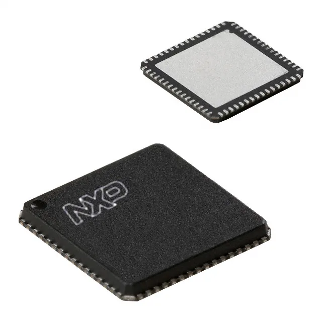
512 KB Flash — firmware budget and field-update headroom
The 512 KB Flash (512K x 8) is sized for a substantial application image plus a bootloader for in-field firmware updates. With 32 KB SRAM, the part can hold moderate data buffers and stack depth for protocol stacks like Modbus RTU or a lightweight TCP/IP offload. The Flash is factory-programmable; no OTP lock means the firmware can be revised during production programming.
Obsolete — sourcing reality and what replaces it
NXP has marked this part as obsolete. Available through surplus and independent-distribution channel.
Mixed-signal I/O — ADC and DAC on one die
Sixteen 10-bit ADC channels and a single 10-bit DAC eliminate the need for external converters in many sensor-front-end and control-output designs. The ADC can sample up to 16 analog inputs (temperature, pressure, current sense) while the DAC provides a single analog setpoint or trim voltage. The internal oscillator further reduces external component count, though an external crystal can be used for tighter timing accuracy.