180 MHz Cortex-M3 — no on-chip Flash
The NXP LPC18S10FET100E is a 32-bit ARM Cortex-M3 MCU clocked at 180 MHz, with 136K x 8 of SRAM and no internal program memory — it is ROMless, so all code must run from external Flash or RAM via the EBI/EMI interface. That makes it a fit for designs where you already have a parallel NOR or NAND Flash on the board and want to avoid duplicating memory. The 180 MHz core gives you headroom for protocol stacks (Ethernet, CAN) or real-time control loops without pushing the bus to its limit.
Connectivity and I/O for industrial control
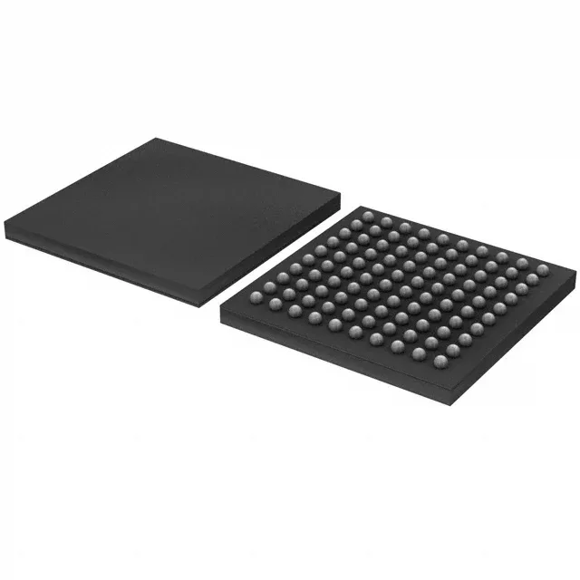
This MCU packs CANbus, I²C, SPI, SSI, SSP, UART/USART, IrDA, Microwire, and MMC/SD interfaces — enough to talk to drives, sensors, and HMI panels over a mix of serial and memory-mapped buses. The 49 general-purpose I/O lines in a 100-TFBGA package (9x9 mm) keep the board footprint tight for space-constrained control modules.
Industrial temperature range, active production
The part is Active in production — no end-of-life notice, no last-time-buy scramble.
Because the LPC18S10FET100E has no internal Flash, the bootloader must reside in external memory — typically a serial NOR Flash or parallel EEPROM on the EBI bus. That adds a memory IC to the BOM but gives you flexibility to change firmware without scrapping the MCU. For field-service swaps, keep a pre-programmed external Flash chip in the kit alongside the MCU; the 100-TFBGA package needs a hot-air station, not a soldering iron, so plan for a rework-capable bench.