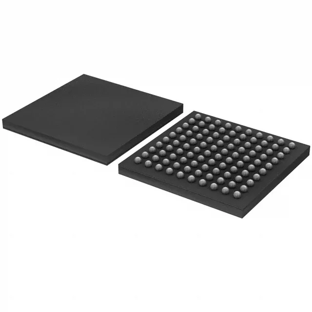
NXP USA Inc. LPC1830FET100Y — Microcontrollers & Processors (MCU / MPU / DSP)

NXP LPC1830FET100Y ARM Cortex-M3 MCU, 180 MHz, ROMless, 100-TFBGA

MPNLPC1830FET100Y
Active

NXP LPC18xx series, ARM Cortex-M3 32-bit single-core MCU, 180 MHz, ROMless, 200K x 8 RAM, 2.2–3.6 V supply, 100-TFBGA (9x9 mm), -40°C to 85°C, Ethernet / CAN / USB OTG / SPI / I²C, 8×10-bit ADC, 1×10-bit DAC, 49 I/O.

$8.2165Ref. price · indicative, final on quote
StockContact for availability
MOQ1 pcs
  • 100% new & originalTraceable channels only — no refurbs, no pulls, no remarked parts.
  • Date & lot codes on quoteStated per line before you commit; label photos on request.
  • MSL-compliant ESD packingMoisture-sealed bags with indicator cards; reels photo-verified.
  • PayPal buyer protectionPay by T/T, PayPal or Payoneer — card payments covered end to end.

Specifications

LPC1830FET100Y Technical Specifications
ParameterValue
SeriesLPC18xx
Mounting typeSurface Mount
Oscillator typeInternal
Program memory typeROMless
Voltage - supply (Vcc (Vdd))2.2V ~ 3.6V
Operating temperature-40°C~85°C(TA)
Speed180MHz
PackageTape & Reel (TR)
RAM size200K x 8
Core size32-Bit Single-Core
PeripheralsBrown-out Detect/Reset, DMA, I²S, POR, WDT
ConnectivityCANbus, EBI/EMI, Ethernet, I²C, IrDA, Microwire, SD, SPI, SSI, SSP, UART/USART, USB, USB OTG
Number of i (O)49
Core processorARM® Cortex®-M3
Case100-TFBGA
Data convertersA/D 8x10b; D/A 1x10b

Product details

180 MHz Cortex-M3 — no internal flash, plan the boot accordingly

The NXP LPC1830FET100Y is a 32-bit ARM Cortex-M3 microcontroller running at 180 MHz, from the LPC18xx series. It is ROMless — there is zero internal flash for program storage — so the design must include an external serial or parallel flash (via the EBI/EMI or SPI/SSP interfaces) for code execution. The 200 KB on-chip SRAM (200K x 8) handles data and can cache critical routines, but the boot vector and main application live off-chip. This architecture suits high-throughput, memory-intensive applications like industrial protocol gateways (Ethernet, CAN, USB OTG are all on-die) or motor-drive control where an external memory bus is already present.

Connectivity set — Ethernet, CAN, USB OTG on one die

The LPC1830FET100Y includes Ethernet, CAN, USB OTG, SPI, I²C, UART, and SSI/SSP interfaces. The EBI/EMI bus connects to external SRAM, NOR flash, or an FPGA.

Package and temperature

The LPC1830FET100Y is in a 100-TFBGA (9x9 mm) package. Operating temperature is -40°C to 85°C. Supply voltage is 2.2 V to 3.6 V.

Sourcing and lifecycle

The LPC1830FET100Y is listed as Active on NXP's product status. It is sourced through independent distribution and quoted to order against an RFQ. Availability and current pricing are confirmed at quote time.

Frequently asked questions

Does LPC1830FET100Y have internal flash memory?

No, the LPC1830FET100Y is ROMless — it has zero internal flash for program storage. Code must execute from an external serial or parallel flash connected via the EBI/EMI or SPI/SSP interfaces.

What is the closest pin-compatible alternative to LPC1830FET100Y?

The NXP LPC1857FET100Y is a pin-compatible alternative in the same 100-TFBGA package: same 180 MHz Cortex-M3 core, but with 1 MB internal flash and 136 KB SRAM. Verify the exact pinout and memory map against your layout before substituting.

What is LPC1830FET100Y's listed speed?

The LPC1830FET100Y is rated for a 180 MHz core clock on the ARM Cortex-M3 processor.

Why is LPC1830FET100Y ROMless?

The LPC1830FET100Y is designed as a ROMless device to give designers flexibility in choosing external memory type and density — suitable for applications that already use an external memory bus and need more code space than internal flash can provide.