The NXP LPC1822JBD144E is a 32-bit ARM Cortex-M3 MCU running at 180 MHz, with 512 KB of Flash program memory and 104 KB of SRAM. The 512 KB Flash and 104 KB SRAM split is sized for a single firmware image with room for field-upgradeable application code and a moderate data buffer — think a servo drive with parameter tables, or a PLC slave node holding a few hundred I/O mapping records. That means you can hang an external SRAM or FPGA on the EBI, talk to a VFD over CAN, and handle USB firmware updates through the same chip — no separate USB controller needed.
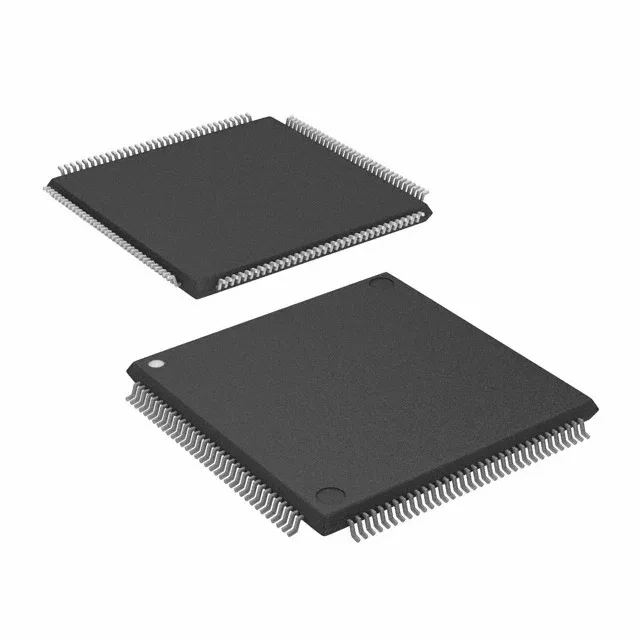
NXP LPC1822JBD144E ARM Cortex-M3 MCU, 180MHz, 512KB Flash
MPNLPC1822JBD144E
Active
NXP LPC18xx series ARM Cortex-M3 32-bit single-core MCU, 180MHz, 512KB Flash, 104KB SRAM, 16KB EEPROM, 83 I/O, 144-LQFP (20×20mm), -40°C to 105°C, 2.2–3.6V supply, USB OTG, CAN, motor control PWM, 8×10b ADC / 1×10b DAC, tray.
$13.3750Ref. price · indicative, final on quote
Independent supplier — new & surplus stockAuthenticity-screened · ESD-safe packingListing updated Jul 2026
Specifications
| Parameter | Value |
|---|---|
| Series | LPC18xx |
| Mounting | Surface Mount |
| Oscillator type | Internal |
| Program memory type | FLASH |
| Voltage - supply (Vcc (Vdd)) | 2.2V ~ 3.6V |
| Operating temperature | -40°C ~ 105°C (TA) |
| Speed | 180MHz |
| Package | Tray |
| RAM size | 104K x 8 |
| Core size | 32-Bit Single-Core |
| EEPROM size | 16K x 8 |
| Peripherals | Brown-out Detect/Reset, DMA, I²S, Motor Control PWM, POR, PWM, WDT |
| Connectivity | CANbus, EBI/EMI, I²C, IrDA, Microwire, SD, SPI, SSI, SSP, UART/USART, USB, USB OTG |
| Number of i (O) | 83 |
| Core processor | ARM® Cortex®-M3 |
| Case | 144-LQFP |
| Data converters | A/D 8x10b; D/A 1x10b |
| Program memory size | 512KB (512K x 8) |
Product details
Frequently asked questions
What is the operating temperature range of LPC1822JBD144E?
The LPC1822JBD144E is rated for -40°C to 105°C, covering industrial and extended-temperature environments.
Does LPC1822JBD144E support USB OTG?
Yes, the LPC1822JBD144E includes USB OTG connectivity alongside CANbus, I²C, SPI, and an external bus interface.
Where can I find the LPC1822JBD144E datasheet and pinout?
The datasheet and pinout for the LPC1822JBD144E are available from NXP's documentation portal; the 144-LQFP pinout follows the standard LPC18xx layout.