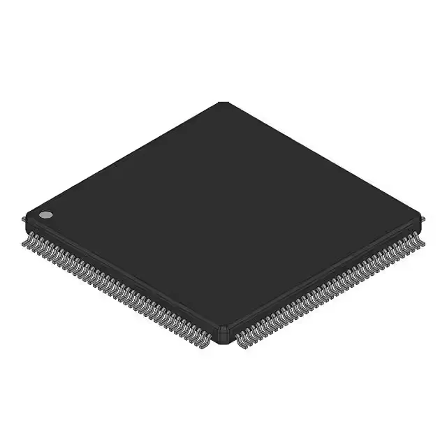
The NXP LPC1813JBD144551 is a 32-bit ARM Cortex-M3 MCU clocked at 180 MHz, with 512 KB of Flash program memory, 104 KB of SRAM, and a separate 16 KB EEPROM block for nonvolatile parameter storage. It runs from a 2.2 V to 3.6 V supply and is rated over the -40°C to 105°C industrial temperature range. On-chip peripherals include a motor-control PWM, DMA, brown-out detection, and watchdog timer. The 180 MHz core speed puts this part in the throughput tier for real-time control loops and protocol stacks — think CANopen master nodes, motor-drive firmware loops, or industrial Ethernet bridges. The integrated 16 KB EEPROM saves an external serial EEPROM for calibration constants or boot parameters, freeing board space and reducing BOM count.
Connectivity and I/O — fits a gateway or drive controller
With CAN, EBI/EMI, and six serial interfaces (I²C, SPI, SSI, SSP, UART, Microwire), this MCU can bridge a CAN fieldbus to an external memory-mapped display or FPGA over the EBI bus without glue logic. The motor-control PWM and DMA engine support sensorless or encoder-based field-oriented control loops — the PWM timers can drive a three-phase inverter bridge, while DMA moves ADC results to RAM without CPU intervention.