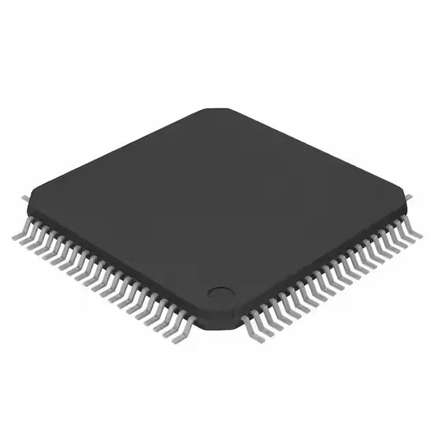
NXP USA Inc. LPC1759FBD80K — Microcontrollers & Processors (MCU / MPU / DSP)

NXP LPC1759FBD80K ARM Cortex-M3 MCU, 120 MHz, 512 KB Flash

MPNLPC1759FBD80K
Active

NXP LPC17xx series, ARM Cortex-M3 32-bit single-core MCU, 120 MHz, 512 KB Flash, 64 KB SRAM, 52 I/O, USB OTG/CAN/SPI/I2C, 2.4–3.6 V, -40 to 85 °C, 80-LQFP (12x12 mm) tray.

$17.2500Ref. price · indicative, final on quote
Independent supplier — new & surplus stockAuthenticity-screened · ESD-safe packingListing updated Jul 2026

Specifications

LPC1759FBD80K specifications
ParameterValue
SeriesLPC17xx
MountingSurface Mount
Oscillator typeInternal
Program memory typeFLASH
Voltage - supply (Vcc (Vdd))2.4V ~ 3.6V
Operating temperature-40°C~85°C(TA)
Speed120MHz
PackageTray
RAM size64K x 8
Core size32-Bit Single-Core
PeripheralsBrown-out Detect/Reset, DMA, I²S, Motor Control PWM, POR, PWM, WDT
ConnectivityCANbus, I²C, IrDA, Microwire, SPI, SSI, SSP, UART/USART, USB OTG
Number of i (O)52
Core processorARM® Cortex®-M3
Case80-LQFP
Data convertersA/D 6x12b SAR; D/A 1x10b
Program memory size512KB (512K x 8)

Product details

120 MHz core and memory budget

The LPC1759FBD80K: The 120 MHz Cortex-M3 core delivers single-cycle multiply and hardware divide, which matters for control-loop math and protocol parsing where every microsecond counts. The 64 KB SRAM supports a few kilobytes of stack and heap plus a pair of DMA buffers; designs that need extensive data logging or large packet buffers should budget RAM carefully.

Housed in an 80-pin LQFP with a 12x12 mm body, the LPC1759FBD80K is a surface-mount part suited for automated assembly on standard PCB processes.

Frequently asked questions

What is the maximum frequency of LPC1759FBD80K?

The LPC1759FBD80K is rated for a 120 MHz core clock.

What is the package of LPC1759FBD80K?

The LPC1759FBD80K is supplied in an 80-pin LQFP package with a 12x12 mm body.

What are the programming interfaces for LPC1759FBD80K?

The LPC1759FBD80K supports in-system programming via its serial interfaces (UART, SPI, I2C) and a dedicated SWD/JTAG debug port, though the exact pin assignments are detailed in the NXP user manual.