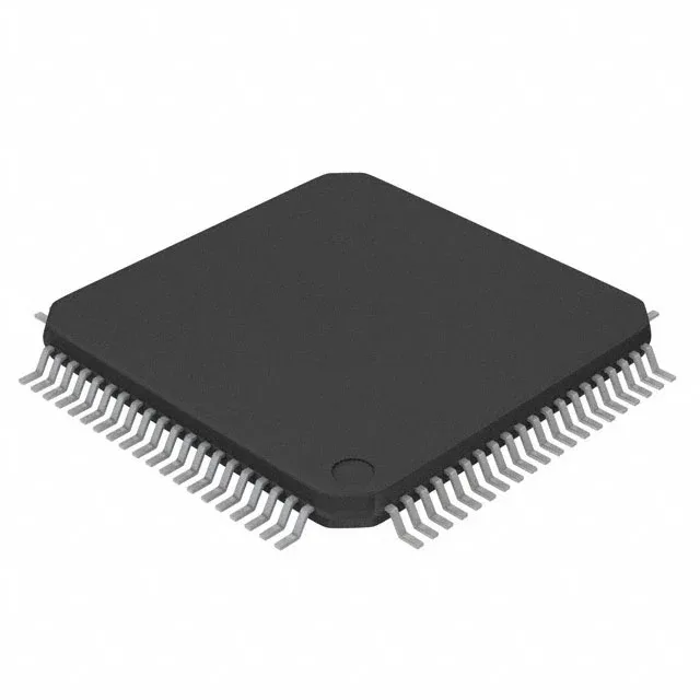
NXP USA Inc. LPC1758FBD80Y — Microcontrollers & Processors (MCU / MPU / DSP)

NXP LPC1758FBD80Y ARM Cortex-M3 MCU, 100MHz, 512KB Flash, 52 I/O — LPC17xx

MPNLPC1758FBD80Y
Active

NXP LPC17xx, LPC1758FBD80Y, ARM Cortex-M3 32-bit single-core 100MHz, 512KB Flash / 64KB RAM, 52 I/O, Ethernet/CAN/USB OTG/I2C/SPI/UART, 6×12-bit ADC + 1×10-bit DAC, 2.4–3.6 V supply, -40 to 85°C, 80-LQFP (12×12mm) surface mount in TR/CT packaging.

$15.1500Ref. price · indicative, final on quote
Packaging80-LQFP
StockContact for availability
MOQ1 pcs
  • 100% new & originalTraceable channels only — no refurbs, no pulls, no remarked parts.
  • Date & lot codes on quoteStated per line before you commit; label photos on request.
  • MSL-compliant ESD packingMoisture-sealed bags with indicator cards; reels photo-verified.
  • PayPal buyer protectionPay by T/T, PayPal or Payoneer — card payments covered end to end.

Specifications

LPC1758FBD80Y Technical Specifications
ParameterValue
SeriesLPC17xx
Mounting typeSurface Mount
Oscillator typeInternal
Program memory typeFLASH
Voltage - supply (Vcc (Vdd))2.4V ~ 3.6V
Operating temperature-40°C ~ 85°C (TA)
Speed100MHz
PackageTape & Reel (TR) Cut Tape (CT)
RAM size64K x 8
Core size32-Bit Single-Core
PeripheralsBrown-out Detect/Reset, DMA, I²S, Motor Control PWM, POR, PWM, WDT
ConnectivityCANbus, Ethernet, I²C, IrDA, Microwire, SPI, SSI, UART/USART, USB OTG
Number of i (O)52
Core processorARM® Cortex®-M3
Case80-LQFP
Data convertersA/D 6x12b; D/A 1x10b
Program memory size512KB (512K x 8)

Frequently asked questions

Is the LPC1758FBD80Y firmware-backward-compatible with an LPC1768 design in Studio 5000?

Both are Cortex-M3 cores in the LPC17xx family and share the same peripheral set layout, but driver-level porting between the LPC1758 and LPC1768 requires a review of the CMSIS headers and LPCOpen software package versions — they are not drop-in firmware interchangeable without a recompile and peripheral driver update.

With 512KB Flash, does the LPC1758FBD80Y justify a longer lead time than the 256KB LPC1754 for a panel BOM of 10 units?

Flash capacity is a design fit question, not a lead-time driver — both parts are in the same NXP family and quoted from the same distribution channel. If the firmware footprint approaches or exceeds 400KB, the 512KB LPC1758 is the correct choice regardless of allocation lead time. For smaller firmware, the LPC1754 is the cost-down alternative.

Can the 6×12-bit ADC on the LPC1758FBD80Y be used simultaneously with the PWM motor-control peripheral without power-cycling the 100MHz core?

The DMA controller (listed in peripherals) handles AHB bus arbitration between the ADC conversion complete flag and the PWM timer triggers, so simultaneous operation is architecturally supported without a core power-down. Hot-swap of sensor channels during live recalibration depends on the specific DMA channel configuration and whether the firmware disables the relevant ADC channel or redirects the DMA stream mid-conversion — a software sequencing question, not a hardware constraint of the MCU.

Does the 1×10-bit DAC meet IEC 61131-2 Type 2 output compliance for ±10 V industrial analog setpoints?

The 10-bit DAC at rail-to-rail output is an on-chip reference-grade converter, not a certified industrial analog output stage. IEC 61131-2 Type 2 compliance for ±10 V signals requires an external precision voltage reference, output amplifier, and fault-protection circuitry — the internal DAC provides the setpoint resolution but not the field-rated output compliance without additional hardware.

What is NXP's PCN status for the 80-LQFP package, and is there a pin-compatible drop-in in the LPC177x series?

No LTB or PCN appears in the current record for the LPC1758FBD80Y. The LPC177x series uses a different pinout and larger package options — it is a functional superset but not a pin-compatible drop-in. A layout change is required to migrate from the 80-LQFP LPC1758 to any LPC177x variant.