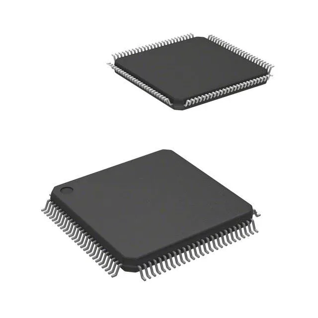
NXP USA Inc. LPC1548JBD100E — Microcontrollers & Processors (MCU / MPU / DSP)

NXP LPC1548JBD100E ARM Cortex-M3 MCU, 72 MHz, 128 KB Flash

MPNLPC1548JBD100E
Active

NXP LPC15xx series ARM Cortex-M3 MCU, 72 MHz, 128 KB Flash, 20 KB RAM, 4 KB EEPROM, 24×12-bit ADC, CANbus, USB, 76 GPIO, 2.4–3.6 V, -40°C to 105°C, 100-LQFP.

$8.4282Ref. price · indicative, final on quote
Independent supplier — new & surplus stockAuthenticity-screened · ESD-safe packingListing updated Jul 2026

Specifications

LPC1548JBD100E specifications
ParameterValue
SeriesLPC15xx
MountingSurface Mount
Oscillator typeInternal
Program memory typeFLASH
Voltage - supply (Vcc (Vdd))2.4V ~ 3.6V
Operating temperature-40°C ~ 105°C (TA)
Speed72MHz
PackageTray
RAM size20K x 8
Core size32-Bit Single-Core
EEPROM size4K x 8
PeripheralsBrown-out Detect/Reset, DMA, POR, PWM, WDT
ConnectivityCANbus, I²C, SPI, UART/USART, USB
Number of i (O)76
Core processorARM® Cortex®-M3
Case100-LQFP
Data convertersA/D 24x12b
Program memory size128KB (128K x 8)

Product details

72 MHz Cortex-M3 with on-chip EEPROM and CANbus

The NXP LPC1548JBD100E is a 32-bit ARM Cortex-M3 MCU running at 72 MHz, with 128 KB Flash, 20 KB RAM, and a separate 4 KB EEPROM block — the EEPROM saves you an external serial memory chip for calibration constants or boot parameters that need to survive a firmware update. On-chip CANbus and USB give it the two most common industrial and debug interfaces without an external transceiver on the USB side (the CAN PHY is still external). The 24-channel 12-bit ADC covers multi-sensor analog front-ends without an external mux.

The 100-LQFP package (14x14 mm body) provides 76 GPIOs.

The DMA engine can service the ADC and serial peripherals without CPU intervention — useful when the 72 MHz core is busy with a control loop or protocol stack. SPI, I²C, and multiple UARTs round out the sensor and actuator interface options.

Lifecycle status is Active — no last-time-buy window, no broker dependency.

Frequently asked questions

What is the closest pin-compatible alternative to LPC1548JBD100E in this component family?

Within the LPC15xx series, pin-compatible density variants share the same 100-LQFP footprint and peripheral set. The LPC1548JBD100E sits at the 128 KB Flash / 20 KB RAM tier; lower-density siblings (e.g., 64 KB Flash) or higher-density options (up to 256 KB Flash) are available if your firmware budget or RAM requirement changes, using the same board layout.

What is LPC1548JBD100E's listed speed (72 MHz) on this component line?

The core runs at 72 MHz — that is the maximum CPU clock for this ARM Cortex-M3 implementation. At that speed the DMA can move ADC results to RAM without stalling the core, and the CANbus controller can handle a 1 Mbps bus load with margin.

What compliance documentation does this brand provide for LPC1548JBD100E (RoHS, REACH, UL, IEC)?

NXP provides RoHS and REACH compliance declarations for the LPC1548JBD100E. The part is lead-free and the 100-LQFP package is compliant with current EU directives. UL and IEC certifications are not typically issued for individual MCUs; system-level safety certification (IEC 61508, ISO 26262) depends on the end application and supporting software libraries.