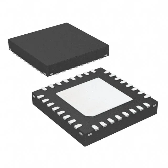
NXP USA Inc. LPC1114FHN33/202,5 — Microcontrollers & Processors (MCU / MPU / DSP)

NXP LPC1114FHN33/202,5 ARM Cortex-M0 MCU, 50 MHz, 32 KB Flash

MPNLPC1114FHN33/202,5
Active

NXP LPC1100L series LPC1114FHN33/202,5, ARM Cortex-M0, 32-bit MCU, 50 MHz, 32 KB Flash, 4K x 8 RAM, 28 I/O, 1.8V-3.6V, -40°C to 85°C, 32-HVQFN (7x7 mm), tray.

$4.8700Ref. price · indicative, final on quote
Packaging32-VQFN Exposed Pad
RoHSROHS3 Compliant
SeriesLPC1100L
Independent supplier — new & surplus stockAuthenticity-screened · ESD-safe packingListing updated Jul 2026

Specifications

LPC1114FHN33/202,5 specifications
ParameterValue
SeriesLPC1100L
MountingSurface Mount
Oscillator typeInternal
Program memory typeFLASH
Voltage - supply (Vcc (Vdd))1.8V ~ 3.6V
Operating temperature-40°C~85°C(TA)
Speed50MHz
PackageTray
RAM size4K x 8
Core size32-Bit Single-Core
PeripheralsBrown-out Detect/Reset, POR, WDT
ConnectivityI²C, SPI, UART/USART
Number of i (O)28
Core processorARM® Cortex®-M0
Case32-VQFN Exposed Pad
Data convertersA/D 8x10b
Program memory size32KB (32K x 8)

Product details

The /202 variant omits the crystal oscillator option and relies on its internal oscillator, saving one external component.

Programming and debug use the standard Serial Wire Debug (SWD) interface — two pins (SWDIO and SWCLK) plus Vcc and GND. Any ARM-compatible debug probe (J-Link, ST-Link, CMSIS-DAP) works. No external crystal is required for SWD because the internal oscillator provides the debug clock.

Frequently asked questions

What is the operating voltage range of LPC1114FHN33/202?

The LPC1114FHN33/202 operates from 1.8V to 3.6V on the Vcc/Vdd supply rail.

What is the closest pin-compatible alternative to LPC1114FHN33/202,5 in this component family?

Within the LPC1114 family, the LPC1114FHN33/302 is pin-compatible but adds an external crystal oscillator option. For designs needing a crystal, the /302 is the direct alternative; for self-clocked designs, the /202 remains the fit.

What is LPC1114FHN33/202,5's listed speed?

The core runs at 50 MHz.

How to program the LPC1114FHN33/202 using SWD?

Connect an SWD debug probe to the SWDIO and SWCLK pins (plus Vcc and GND). The internal oscillator provides the debug clock, so no external crystal is needed. Any ARM-compatible probe such as J-Link or CMSIS-DAP works with Keil MDK or NXP's MCUXpresso IDE.