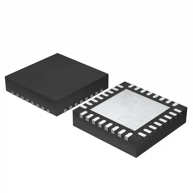
NXP USA Inc. LPC1114FHI33/302,5 — Microcontrollers & Processors (MCU / MPU / DSP)

NXP LPC1114FHI33/302,5 ARM Cortex-M0 MCU, 50 MHz, 32 KB Flash

MPNLPC1114FHI33/302,5
Active

NXP LPC1114FHI33/302,5, ARM Cortex-M0 32-bit MCU, 50 MHz, 32 KB Flash, 8 KB RAM, 28 I/O, I²C/SPI/UART, 1.8-3.6 V, -40 to 85°C, 32-HVQFN (5x5 mm).

$4.6300Ref. price · indicative, final on quote
Independent supplier — new & surplus stockAuthenticity-screened · ESD-safe packingListing updated Jul 2026

Specifications

LPC1114FHI33/302,5 specifications
ParameterValue
SeriesLPC1100L
MountingSurface Mount
Oscillator typeInternal
Program memory typeFLASH
Voltage - supply (Vcc (Vdd))1.8V ~ 3.6V
Operating temperature-40°C ~ 85°C (TA)
Speed50MHz
PackageTray
RAM size8K x 8
Core size32-Bit Single-Core
PeripheralsBrown-out Detect/Reset, POR, WDT
ConnectivityI²C, SPI, UART/USART
Number of i (O)28
Core processorARM® Cortex®-M0
Case32-VFQFN Exposed Pad
Data convertersA/D 8x10b
Program memory size32KB (32K x 8)

Product details

What this Cortex-M0 MCU brings to the board

The NXP LPC1114FHI33/302,5 is a 32-bit ARM Cortex-M0 microcontroller from the LPC1100L series, clocked at 50 MHz with 32 KB of Flash program memory and 8 KB of RAM. It packs 28 general-purpose I/O lines and a set of serial interfaces — I²C, SPI, and UART/USART — plus an 8-channel 10-bit ADC, all in a compact 32-HVQFN package measuring 5x5 mm. The supply range spans 1.8 V to 3.6 V, and the operating temperature covers -40°C to 85°C, making it suitable for industrial control, sensor nodes, and embedded I/O modules where board space is tight and the environment is not climate-controlled.

The 50 MHz clock on this Cortex-M0 handles a PID loop update every few microseconds. Brown-out detection and watchdog are built in as peripherals.

Memory sizing for production firmware

32 KB of Flash and 8 KB of RAM fit a small RTOS and serial protocol handler. The 8 KB RAM is shared between stack, heap, and ADC buffer.

The 32-HVQFN package with an exposed pad helps thermal transfer to the PCB copper pour — useful if the MCU is driving I/O near the maximum 28 pins.

Frequently asked questions

What is the pinout and package footprint of LPC1114FHI33/302?

The package is a 32-HVQFN with an exposed pad, 5x5 mm body. The pinout is standard for the LPC1114 family; the base product number LPC1114 shares the same footprint across density variants.

What programmer or debugger supports LPC1114FHI33/302?

Standard ARM Cortex-M0 debug probes (JTAG/SWD) work with this MCU. Common choices include the NXP LPC-Link2, Segger J-Link, and CMSIS-DAP based adapters.

What is the difference between LPC1114FHI33/302 and LPC1114FHI33/302E?

The 'E' suffix typically indicates an extended temperature range or a different revision. For exact differences, compare the datasheet markings; the base LPC1114 family shares the same pinout and memory map.