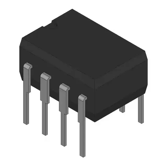
Analog Devices TSC427EPA

TSC427EPA Dual MOSFET Driver, 1.5A Peak, 20ns, 8-DIP

MPNTSC427EPA
End of Life

TelCom Semiconductor TSC427EPA dual low-side MOSFET driver, 1.5A peak output, 20ns typ rise/fall, 4.5V to 18V supply, non-inverting, independent channels, through-hole 8-DIP (0.300", 7.62mm) package.

$2.0Ref. price · indicative, final on quote
Packaging8-DIP (0.300", 7.62mm)
StockContact for availability
MOQ1 pcs
  • 100% new & originalTraceable channels only — no refurbs, no pulls, no remarked parts.
  • Date & lot codes on quoteStated per line before you commit; label photos on request.
  • MSL-compliant ESD packingMoisture-sealed bags with indicator cards; reels photo-verified.
  • PayPal buyer protectionPay by T/T, PayPal or Payoneer — card payments covered end to end.

Specifications

TSC427EPA Technical Specifications
ParameterValue
Gate typeN-Channel, P-Channel MOSFET
Input typeNon-Inverting
Channel typeIndependent
Mounting typeThrough Hole
Voltage4.5V ~ 18V
Logic voltage - VIL, VIH0.8V, 2.4V
Current - peak output (Source, sink)1.5A, 1.5A
PackageBulk
Case8-DIP (0.300\", 7.62mm)
Number of drivers2
Driven configurationLow-Side
Rise (Fall time)20ns, 20ns

Product details

Dual low-side MOSFET driver — 1.5 A peak, 20 ns edges

The TelCom Semiconductor TSC427EPA is a dual low-side MOSFET driver for N-channel and P-channel power MOSFETs. Each of the two independent, non-inverting channels delivers 1.5 A peak source and 1.5 A peak sink current, with typical rise and fall times of 20 ns. The supply range spans 4.5 V to 18 V. Logic inputs are compatible with standard CMOS and TTL levels — VIL at 0.8 V, VIH at 2.4 V.

Where it fits — switching loads and gate-drive circuits

This driver is sized for applications that need to switch a pair of low-side MOSFETs at moderate frequency: DC-DC converters, motor-drive half-bridges, solenoid drivers, and class-D audio output stages. The 1.5 A peak output can charge and discharge the gate capacitance of a medium-power MOSFET in tens of nanoseconds, keeping switching losses in check. The through-hole package (0.300" width, 7.62 mm pitch) is a standard footprint for prototyping, legacy board rework, and designs where through-hole assembly is preferred over surface-mount.

Active lifecycle — no obsolescence risk for new builds

The TSC427EPA carries an active product status. For a BOM line that needs a dual low-side driver in an 8-pin DIP, this part is a straightforward fit for both new designs and ongoing production — no supply-chain clock ticking.

RoHS note — verify compliance requirements

This part is listed as RoHS non-compliant. If your assembly process or end-market requires RoHS exemption or full compliance, confirm the solder-joint and material restrictions before committing the BOM.

Frequently asked questions

What is the difference between TSC427EPA and TSC428EPA?

The TSC428EPA is the inverting version of this driver family. The TSC427EPA is non-inverting — a logic high on the input turns the output high. The TSC428EPA inverts that relationship. Both share the same pinout, package, and 1.5 A peak output rating, so the choice depends on whether your PWM controller or logic output needs an inversion or not.

Can TSC427EPA drive both N-channel and P-channel MOSFETs?

Yes. The TSC427EPA is specified for driving both N-channel and P-channel MOSFETs. The low-side configuration and non-inverting input work with either channel type, as long as the gate threshold and gate charge are within the driver's 1.5 A peak output and 4.5 V to 18 V supply range.