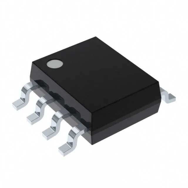
Analog Devices TSC427CBA+ — Logic ICs

TSC427CBA+ Low-Side MOSFET Gate Driver, 1.5A, 8-SOIC

MPNTSC427CBA+
End of Life

Maxim Integrated TSC427CBA+ low-side MOSFET gate driver, 2 independent channels, 1.5A peak source/sink, 25ns typ rise/fall, 4.5V–18V supply, 8-SOIC package, 0°C to 70°C.

$7.0Ref. price · indicative, final on quote
Packaging8-SOIC (0.154", 3.90mm Width)
StockContact for availability
MOQ1 pcs
  • 100% new & originalTraceable channels only — no refurbs, no pulls, no remarked parts.
  • Date & lot codes on quoteStated per line before you commit; label photos on request.
  • MSL-compliant ESD packingMoisture-sealed bags with indicator cards; reels photo-verified.
  • PayPal buyer protectionPay by T/T, PayPal or Payoneer — card payments covered end to end.

Specifications

TSC427CBA+ Technical Specifications
ParameterValue
Gate typeN-Channel, P-Channel MOSFET
Input typeNon-Inverting
Channel typeIndependent
Mounting typeSurface Mount
Voltage4.5V ~ 18V
Logic voltage - VIL, VIH0.8V, 2.4V
Current - peak output (Source, sink)1.5A, 1.5A
Operating temperature0°C ~ 70°C (TA)
PackageTube
Case8-SOIC (0.154\", 3.90mm Width)
Number of drivers2
Driven configurationLow-Side
Rise (Fall time)25ns, 25ns

Product details

The 4.5V to 18V supply range lets it operate from a 5V logic rail or a 12V industrial bus, though the low end of that range needs checking against the MOSFET's Vgs threshold.

Package and mounting

The 1.5A source/sink rating determines how fast the driver can charge and discharge the MOSFET gate capacitance. A 1.5A peak into a 10 nC total gate charge (typical for a small TO-220 MOSFET) yields a transition time around 6–7 ns, well within the 25 ns typical rise/fall window. That keeps crossover conduction losses low in a half-bridge, but the designer still needs to budget dead time from the controller side — the driver itself has no built-in cross-conduction prevention. For larger dies (100 nC gate charge or more), the 1.5A peak will stretch the switching edge; consider a higher-current driver if the application runs above 200 kHz.

Supply range and logic thresholds

The 4.5V to 18V supply range covers the common 5V and 12V rails. The logic input thresholds are 0.8V (VIL) and 2.4V (VIH), so a 3.3V logic output will drive it cleanly as long as the high-level voltage exceeds 2.4V — most 3.3V CMOS outputs do, but check the actual VOH at the source current. At the low end of the supply range (4.5V), the gate drive voltage to the MOSFET is only about 4.5V, which may not fully enhance a standard-threshold MOSFET; logic-level or sub-logic-level MOSFETs are the right match here.

Frequently asked questions

Can TSC427CBA+ replace TC427?

The TSC427CBA+ is a direct functional equivalent to the TC427 — same dual low-side driver, same 1.5A peak output, same 8-SOIC footprint. The pinout is identical, so it is a drop-in replacement for the TC427 in existing designs.

Can TSC427CBA+ drive both N-channel and P-channel MOSFETs?

Yes, the gate type is specified for both N-channel and P-channel MOSFETs. The driver outputs are non-inverting and independent, so each channel can drive either polarity as long as the supply and ground references are correct for the MOSFET configuration.