28:1 serializer at 3.12 Gbps — what the data rate means for the link
The MAX9275GTN/V+T is a 28-input, 1-output serializer from Analog Devices, part of their GMSL (Gigabit Multimedia Serial Link) family. It takes 28 parallel LVCMOS inputs and serializes them onto a single CML output at up to 3.12 Gbps — that is the raw bit rate on the serial line, not the payload throughput. At 3.12 Gbps, the serial stream carries 28 bits per pixel clock cycle, so the effective parallel-side pixel clock is 3.12 Gbps ÷ 28 = ~111 MHz. If your camera or display interface runs a pixel clock above that, the serializer cannot keep up — the 3.12 Gbps figure sets the ceiling on the parallel input rate, not just the cable speed.
Supply rails and temperature — industrial-automotive crossover
This is not the full under-hood 125°C grade, but it suits camera modules behind the windshield or inside an IP65-rated housing on a factory floor.
56-TQFN package — thermal and layout notes
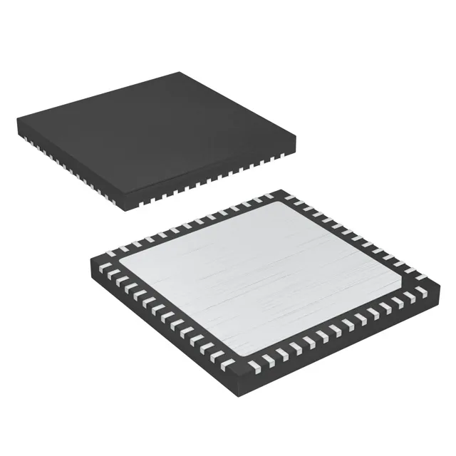
The 56-WFQFN exposed-pad package (8x8 mm, 0.5 mm pitch) has a large thermal pad on the bottom. For a 3.12 Gbps CML output, the differential trace pair should be 100 Ω controlled impedance, with the ground plane directly under the package pad to minimise the loop area. The 0.5 mm pitch means a 4-layer board is practical for fan-out; a 2-layer board will struggle to route all 28 LVCMOS inputs without vias.