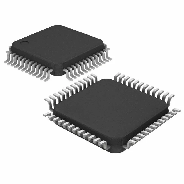
LVDS deserializer with a 27-bit parallel bus
The MAX9218ECM+ is a single-channel LVDS deserializer that converts a 700 Mbps serial stream back into a 27-bit-wide LVCMOS or LVTTL parallel bus. That 27-output count tells you the link carries pixel data, control lines, and a clock — typical for a TFT panel or a multi-sensor aggregator where the serializer on the far end packs everything into one differential pair. The 48-pin LQFP footprint is a standard fine-pitch quad flat pack — the 0.5 mm pitch demands careful fan-out on a two-layer board, but a four-layer stack-up with a dedicated ground plane under the package gives clean signal integrity at 700 Mbps.
What the 700 Mbps data rate means for your link budget
700 Mbps is the serial line rate on the LVDS pair. The deserializer recovers the embedded clock and presents the parallel data on 27 outputs — the effective pixel clock or parallel bus frequency is 700 Mbps divided by 27, roughly 25.9 MHz. That is fast enough for a 640x480 display at 60 Hz with some overhead, or for aggregating multiple lower-speed sensor streams into one cable. The LVDS input uses a 100-ohm differential termination — the receiving end expects the pair to be terminated at the deserializer pins, not at the connector. If your board layout runs the LVDS pair through a connector, place the termination resistor within 5 mm of the MAX9218ECM+ pins to avoid reflections that close the eye diagram at 700 Mbps. Outputs are LVCMOS or LVTTL, selectable per the supply rail — at 3.3 V they swing LVTTL levels; at 3.0 V they are LVCMOS. The 27 outputs drive parallel loads up to the standard 15 pF per pin at 25 MHz; exceeding that capacitance stretches the rise time and may violate the setup time of the downstream FPGA or ASIC.
Package, supply, and temperature — the board-fit checklist
A 2x2 array of thermal vias under the pad, connected to an inner-layer ground plane, drops the thermal resistance by roughly 30% compared to a pad with no vias. The part draws its quiescent current from this single rail — no separate analog or PLL supply needed. Decouple with a 0.1 µF ceramic placed as close to each VDD pin as the LQFP pitch allows, plus a 10 µF bulk capacitor within 10 mm. The Tray package is the standard shipping medium for LQFP devices — 160 units per tray, JEDEC-compliant. For reflow, the moisture sensitivity level (MSL) is typically MSL 3 for this package family, meaning a 168-hour floor life after the bag is opened. Bake at 125°C for 24 hours if the floor life is exceeded.
Active production and compliance status
Because it is an active, current-production part, it is available through authorized distribution channels.