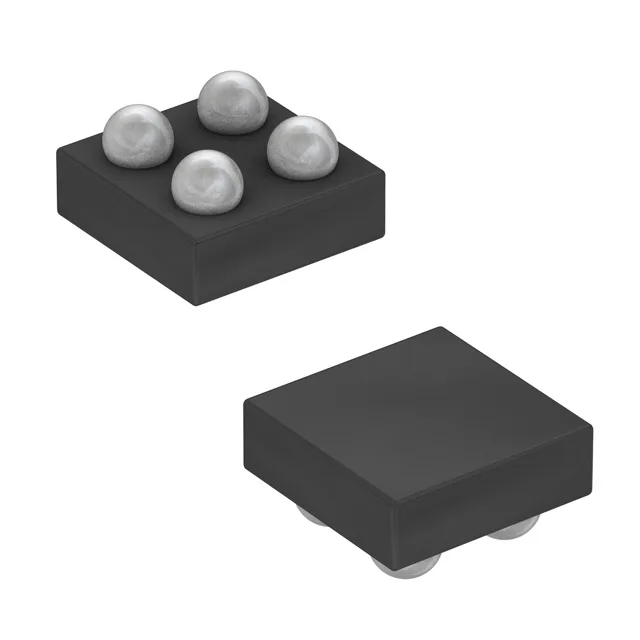
Analog Devices MAX9063EBS+TG45 — Analog & Data Acquisition

MAX9063EBS+TG45 Comparator with Voltage Reference, 1.1 µA

MPNMAX9063EBS+TG45
End of Life

Analog Devices MAX9063EBS+TG45 single comparator with integrated voltage reference, 1.1 µA quiescent current, open-drain output, ±12 mV hysteresis, 4-UCSP (1.05x1.05 mm) package, Tape & Reel.

$1.47Ref. price · indicative, final on quote
Packaging4-WFBGA, CSPBGA
StockContact for availability
Lead timeIn Stock wk
MOQ1 pcs
  • 100% new & originalTraceable channels only — no refurbs, no pulls, no remarked parts.
  • Date & lot codes on quoteStated per line before you commit; label photos on request.
  • MSL-compliant ESD packingMoisture-sealed bags with indicator cards; reels photo-verified.
  • PayPal buyer protectionPay by T/T, PayPal or Payoneer — card payments covered end to end.

Specifications

MAX9063EBS+TG45 Technical Specifications
ParameterValue
Typewith Voltage Reference
Output typeOpen-Drain
Mounting typeSurface Mount
Voltage - supply, single (Dual (±))1V ~ 5.5V
Current - quiescent1.1µA
Current - input bias60pA @ 3.3V
Operating temperature-40°C ~ 85°C
PackageTape & Reel (TR); Cut Tape (CT)
Hysteresis±12mV
Case4-WFBGA, CSPBGA
CMRR, PSRR53dB PSRR
Number of elements1
Propagation delay15µs

Product details

Ultra-low-power comparator with onboard reference in 1 mm²

The MAX9063EBS+TG45 from Analog Devices integrates a single comparator with a voltage reference in a 4-UCSP package measuring just 1.05 mm x 1.05 mm — the reference and comparator share one die, so the threshold is set without external resistors or a separate reference IC.

Built-in hysteresis kills the chatter

±12 mV of internal hysteresis means the comparator does not oscillate near the threshold — an op-amp pressed into comparator service would need external positive feedback to match this, and the MAX9063 already has it on-chip. Propagation delay is 15 µs maximum — fast enough to catch a 33 kHz signal edge cleanly, but not a high-speed pulse train. The open-drain output lets the user pull up to any voltage up to the supply rail, making it straightforward to interface a 1.8 V sensor threshold to a 3.3 V logic input. Input bias current is 60 pA maximum at 3.3 V — negligible for a 10 MΩ sensor divider, where the bias-induced offset stays under 600 µV. Power-supply rejection ratio is 53 dB typical, so a 100 mV ripple on the supply rail shifts the threshold by roughly 0.2 mV — the internal reference tracks supply changes well enough that the trip point stays stable without a separate LDO.

Frequently asked questions

Is MAX9063EBS+TG45 compatible with 3.3 V systems?

The open-drain output pulls up to any voltage up to the supply rail, making the interface to 3.3 V logic direct.

What is the footprint for MAX9063EBS+TG45?

The supplier device package is 4-UCSP measuring 1.05 mm x 1.05 mm. It is a 4-ball WFBGA/CSPBGA — the PCB land pattern follows the JC-42 standard for 0.50 mm pitch CSP. A solder-mask-defined pad is recommended for reliable assembly.