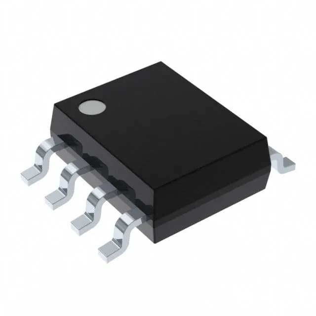
Negative rail from a positive supply — the charge pump approach
The MAX889TESA+ from Maxim Integrated is a charge-pump-based step-down regulator that generates a regulated negative output voltage from a positive input rail. It delivers up to 200 mA of output current and switches at 2 MHz, which keeps the external flying and reservoir capacitors small — typically 1 µF to 10 µF ceramic types. The input range spans 2.7 V to 5.5 V, so it can run from a single Li-ion cell, a 3.3 V rail, or a 5 V rail. The output is adjustable from -2.5 V down to -5.5 V, making it a fit for generating a negative bias rail in op-amp circuits, LCD bias supplies, or GaN FET gate drivers that need a clean negative voltage.
What the 200 mA output means for your load budget
The 200 mA rating is the maximum continuous output current. For a negative rail powering a handful of op-amps, a small LCD bias, or a low-power RF switch, this is ample. If your load draws close to the limit, factor in the charge pump's efficiency — at 200 mA the input current will be roughly 1.5× to 2× the output current, depending on input-to-output voltage ratio. The 2 MHz switching means the ripple frequency is high enough that a small LC post-filter can knock it down to low-noise levels, which is relevant if the rail feeds sensitive analog circuitry.
Temperature grade and deployment environment
Rated for -40°C to 85°C, the MAX889TESA+ suits industrial control, outdoor telecom, and automotive cabin environments where the ambient temperature stays within that band. No synchronous rectifier means the charge pump uses diode-based switching — fine for this current level, but the forward drop of the external Schottky diode adds to the dropout. At cold temperatures the diode drop increases slightly, so budget an extra 100 mV or so on the dropout margin.
Package and footprint — 8-SOIC
The part comes in an 8-SOIC package, a widely used surface-mount footprint that is easy to hand-solder and inspect. The supplier device package is 8-SOIC. The shipping medium is Tube. The 8-SOIC body is 3.90 mm wide, which fits standard SOIC-8 land patterns. No exposed pad, so thermal dissipation relies on the copper traces and the board itself — at 200 mA continuous output, keep the ambient under 70°C if the board has limited copper area.
Lifecycle and sourcing
The MAX889TESA+ carries an Active lifecycle status and is ROHS3 compliant. The active status means no imminent supply risk for production builds.