Noise rejection across the audio band — what the PSRR curve means
The MAX8840ELT33+T: The PSRR is specified at 78 dB at 1 kHz, rolling off to 54 dB at 100 kHz. Above 100 kHz the rejection drops, so if the upstream supply is a switching converter running at 500 kHz, the LDO alone won't clean that noise; a post-filter LC stage before the LDO input is the usual fix. The 90 µA quiescent current is the LDO's own draw — it stays constant across load, so on a battery-powered sensor that sleeps most of the time, that 90 µA is the dominant drain when the load is off. For a 100 mAh coin cell, the LDO alone pulls about 46 days of standby before the load even wakes.
Dropout and headroom — the input rail must stay above 3.42 V
The dropout voltage is 120 mV typical at 120 mA load. That means the input rail must stay above 3.42 V (3.3 V + 0.12 V) to keep the output in regulation at that current. At lighter loads the dropout is lower, but the design rule is: if the input rail dips below 3.42 V under full load, the output follows it down. The max input is 6 V, so a 5 V rail is fine; a 3.6 V lithium cell near end-of-discharge (3.0 V) won't hold regulation. That's useful for sequencing: the MCU can hold the analog rail off until the system is ready to sample, then assert enable and wait for the output to settle.
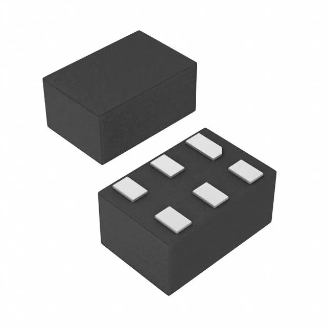
Package and board-fit — 6-uDFN, 1.5 mm × 1.0 mm
For 150 mA output at 3.3 V from a 5 V input, the LDO dissipates about 255 mW (1.7 V drop × 150 mA). The 6-WFDFN footprint is common — no exotic pad geometry — so reflow profiles for standard lead-free solder work. No moisture sensitivity level is listed, but for a small leadless package, a bake before reflow is cheap insurance if the reel seal is broken.