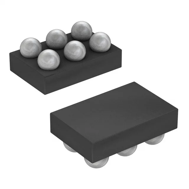
Package and board-fit: 6-WLP with 1.22x0.85 mm footprint
The MAX77324EWTAD+T comes in a 6-WFBGA, WLBGA package, with the supplier device package specified as 6-WLP (1.22x0.85). This is a wafer-level package — the die itself is the package, with solder bumps directly on the active surface. The 0.85 mm narrow side means the part fits into tight edge-of-board or module spaces where a larger QFN would not clear. Surface-mount assembly is standard, but the 0.4 mm typical ball pitch on a WLP demands a solder-mask-defined pad with a 0.25 mm opening and a stencil aperture matched to the ball diameter. The board-side copper pad should be non-solder-mask-defined (NSMD) to keep the solder joint consistent across reflow.
Input and output voltage envelope
Because the output is PWM-controlled and the part integrates a synchronous rectifier, the efficiency stays high across the load range — the rectifier replaces the external Schottky diode, cutting the forward-drop loss that a non-synchronous buck would incur at low output voltages.
Rated for 1.5 A continuous output current, this regulator can supply a small MCU core plus a few peripheral loads without needing an external pass transistor. The 2 MHz switching frequency pushes the fundamental ripple above the audio band and lets the designer use a 1 µH or smaller inductor — the inductor ripple current at 2 MHz is roughly one-third of what it would be at 600 kHz, so the output capacitor can be a 10 µF ceramic instead of a bulkier tantalum. The trade-off at 2 MHz is higher switching losses in the internal FETs — at light loads (below 100 mA) the efficiency drops compared to a 1 MHz part, but for a 500 mA to 1.5 A load the 2 MHz part wins on inductor and capacitor size.
The part is not rated for automotive (AEC-Q100) or extended industrial (105°C or 125°C), so it fits indoor equipment, portable devices, and telecom gear that stays within a conditioned or sheltered environment. The WLP package has a junction-to-board thermal resistance around 50-60°C/W typical for a 6-ball array. At 1.5 A output and 3.3 V to 1.8 V conversion (about 2.25 W input, 2.7 W output — roughly 0.45 W dissipated in the regulator), the junction temperature rise above the board is about 25-30°C. With a 85°C ambient, the junction stays below 115°C, well within the silicon limit.
ROHS3 compliant, so it meets the current EU RoHS exemption rules including the updated phthalates restriction. If the BOM requires a second source, a parametric search for a 6-WLP step-down buck with 1.5 A output, 2 MHz switching, and 2.5-4.8 V input range would yield candidates from other vendors, but the WLP footprint is vendor-specific — a board spin would be needed for a different package.