What the 2A peak output and 25ns edge rate mean for your gate drive
The MAX627CPA+ delivers 2A peak source and 2A peak sink current — enough to charge and discharge the gate capacitance of a medium-power MOSFET or IGBT in the 10-50 nC range within the typical 25ns rise and 20ns fall times. That edge rate means the driver can switch a 10 nF gate load from 0 to 12V in about 60 ns, keeping switching losses low in a 100-200 kHz SMPS or motor-drive stage. The non-inverting input simplifies the control logic — a high on the input turns the output on directly, no extra inversion stage needed in the PWM path. Logic thresholds at 0.8V VIL and 2.4V VIH are TTL-compatible, so the driver interfaces cleanly with 3.3V or 5V controllers without a level translator.
Supply range, temperature grade, and package fit
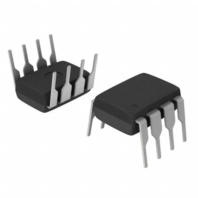
Operating from 4.5V to 18V, the driver covers standard logic and bias rails — a 5V or 12V supply both work, and the 18V ceiling accommodates automotive pre-regulator rails. Housed in an 8-DIP (0.300", 7.62mm) through-hole package with the 8-PDIP supplier device code, it fits standard prototyping breadboards and socketed production boards — no reflow profile needed. The independent channel architecture lets each of the two drivers operate with separate gate resistors and return paths, useful for driving a half-bridge where the high-side bootstrap needs its own timing.
Lifecycle and compliance snapshot
RoHS3 compliant, with no lead, mercury, cadmium, or other restricted substances above the threshold — acceptable for EU and global markets without an exemption claim.