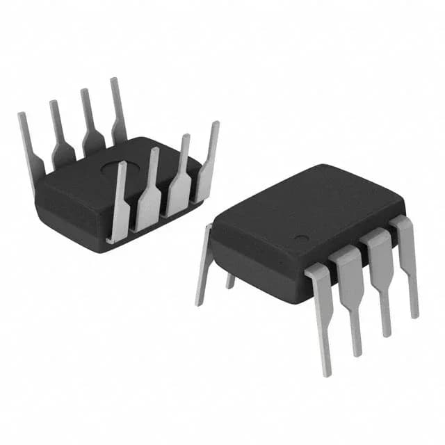
Dual 2A low-side driver for N- and P-channel MOSFETs
The Maxim Integrated MAX626CPA+ is a dual-channel, low-side MOSFET gate driver designed to drive both N-channel and P-channel MOSFETs. Each of the two independent drivers delivers a peak output current of 2A source and 2A sink, with typical rise and fall times of 25ns and 20ns respectively — fast enough to minimize switching losses in 500kHz+ power converters without excessive shoot-through. The inverting input logic accepts standard CMOS/TTL levels (VIL 0.8V, VIH 2.4V) across a supply range of 4.5V to 18V, making it a natural fit for 5V or 12V gate-drive rails in industrial power supplies, DC-DC modules, and motor-drive pre-drive stages. The through-hole 8-DIP package (0.300" body) suits prototype builds, low-volume production, and retrofit upgrades where a socketed driver is preferred.
2A peak drive — what it means for your MOSFET selection
The 2A peak source and sink current rating determines how quickly the driver can charge and discharge the MOSFET gate capacitance. For a typical power MOSFET with 10 nC total gate charge at 12V, the 2A peak translates to roughly 5 ns of gate-drive rise time — well within the 25ns typical rise spec. This driver comfortably handles MOSFETs with gate charges up to about 50 nC without significant slowdown. If your design uses larger dies (e.g., TO-247 packages with 100 nC+ gate charge), the switching edges will stretch, and you may need to budget additional dead-time or consider a higher-current driver. The independent channel architecture lets you drive two separate MOSFETs with independent control signals — useful for synchronous buck converters where the high-side and low-side switches need separate drive paths, though note this is a low-side driver only, so the high-side MOSFET in a half-bridge requires a bootstrap or isolated supply.
Supply range and logic compatibility
The 4.5V to 18V supply range covers the two most common gate-drive voltages: 5V for logic-level MOSFETs and 12V for standard-threshold power MOSFETs. The inverting input means the output goes high when the input is low — a detail that matters when interfacing to a PWM controller with active-high outputs; you may need an external inverter or choose the non-inverting variant (MAX627). The logic thresholds (VIL 0.8V, VIH 2.4V) are compatible with 3.3V and 5V logic families, but at 3.3V VOH the margin above VIH is only 0.9V — keep the input trace short and clean to avoid false triggering. The operating temperature range of 0°C to 70°C limits this part to commercial/indoor equipment; for industrial or automotive environments, look at the industrial-temperature MAX626CPA+ variant or the MAX627/MAX628 family.
Lifecycle and sourcing
For dual-sourcing resilience, the pin-compatible MAX627CPA+ (non-inverting input) and MAX628CPA+ (dual-input with enable) are direct functional alternatives within the same family — though verify the input logic polarity matches your controller.