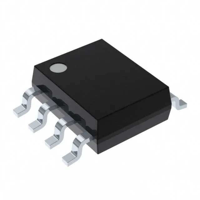
Fixed 5V series reference with ±0.02% accuracy
The MAX6126AASA50+T is a precision series voltage reference from Analog Devices that outputs a fixed 5V with an initial tolerance of ±0.02%. That ±1 mV maximum error at 25°C is tight enough to feed a 12-bit ADC without external calibration — the reference error budget is well under 1 LSB for a 5V full-scale input. Temperature drift is specified at 5 ppm/°C. Over the full -40°C to +125°C industrial range, that translates to roughly 25 ppm total drift, or 125 µV on the 5V output — a 16-bit ADC sees that as about 1.6 LSB of drift, which is acceptable for most industrial measurement chains. Low-frequency noise from 0.1 Hz to 10 Hz is 2.85 µVp-p. This is the noise that integrates over the conversion time of a delta-sigma ADC; at this level, the reference noise does not dominate the ADC's noise floor, preserving the system's effective resolution.
Supply range and output drive
Input voltage range is 5.2V to 12.6V. The 200 mV headroom above the 5V output is the minimum dropout; if the input rail is noisy or droops below 5.2V, the output accuracy degrades. A clean 5.5V to 6V rail is a safe operating point. Output current is rated at 10 mA. This can drive one or two ADC reference inputs directly — typical SAR ADC reference draw is 1-2 mA. If the load exceeds 10 mA, an external buffer is required. Supply current consumption is 725 µA, which is the quiescent current drawn from the input rail regardless of load.
Active lifecycle and sourcing posture
No end-of-life notice or successor has been issued. The part is supplied in Tape & Reel (TR) or Cut Tape (CT) format, in an 8-SOIC package with 0.154-inch body width.