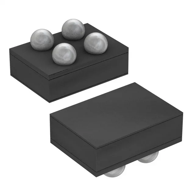
WLP footprint and reflow considerations
The MAX6069CAAWS+T comes in a 4-WFBGA, WLBGA package (supplier device package 4-WLP, 1.16x0.88 mm). That is a wafer-level chip-scale package with solder balls directly on the die — no molded body. The pad pitch is tight, and the package sits flush on the board with a near-zero standoff. Reflow profile must follow the JEDEC J-STD-020 moisture sensitivity level for the part; if the MSL rating is Level 1, it survives the oven without a bake. If it is Level 2 or higher, skipping the pre-reflow bake risks popcorning — the trapped moisture expands and lifts the die off the balls. Surface-mount placement on a standard 4-ball WLP footprint. The 0.88 mm width means the pick-and-place nozzle needs a small vacuum cup — a standard 8 mm nozzle may overlap the edge and lose grip. Stencil aperture should match the ball diameter for consistent solder volume; too much paste and the part floats, too little and the joint opens under thermal cycling.
Precision and noise floor for the reference rail
Fixed 2.5 V output with ±0.2% initial tolerance — that is ±5 mV at 25 °C. For a 12-bit ADC with a 2.5 V reference, this error eats about 2 LSBs of the full-scale budget before the converter's own INL. The 25 ppm/°C temperature coefficient adds another 1.25 mV drift over the -40 to +125 °C range, so the total reference error across temperature stays under 0.25%. That flicker-noise floor sets the practical resolution limit for a DC measurement system using this reference — below about 16 bits the noise is buried in the quantization error; at 18 bits it starts to limit the effective number of bits. As a shunt reference, it draws 2 mA supply current — the current through the external resistor sets the operating point. The shunt topology means it can sink or source current, so it regulates a load that both draws and returns current, unlike a series reference.