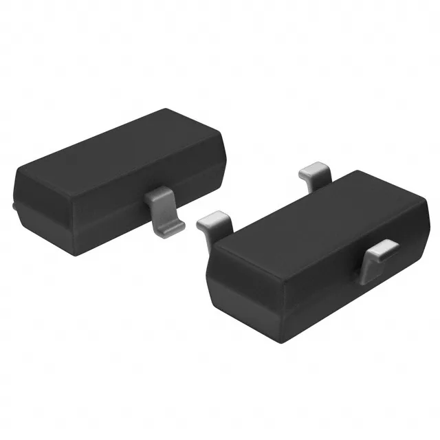
Precision 4.096V reference for ADC/DAC bias and measurement chains
The MAX6064AEUR+T: This output voltage is a standard full-scale reference for 12-bit and 16-bit successive-approximation ADCs — the 4.096 V rail maps directly to a 1 mV LSB in a 12-bit system, simplifying the gain calculation in the signal chain. For a system that sees a 50 °C swing, the total drift contribution from the reference is roughly 0.1% — well within the error budget of a 12-bit measurement without calibration.
In a 16-bit ADC with a 4.096 V reference, the LSB is 62.5 µV — the peak-to-peak noise in the sub-10 Hz band sits just under one LSB, so the reference itself does not dominate the noise floor in precision DC measurements. The 5 mA output current capability is enough to bias the reference input of a single ADC or DAC, plus a small resistive divider for scaling. The 125 µA quiescent supply current means the reference adds negligible overhead to the system power budget in battery-powered or loop-powered designs.
SOT-23-3 footprint and industrial temperature grade
The series reference topology means the output is actively buffered — it does not require an external load resistor to maintain regulation, unlike a shunt reference. The input capacitor and output bypass capacitor recommended in the datasheet are the only external components needed for stable operation.