Analog Devices MAX5531ETC+ — Analog & Data Acquisition

MAX5531ETC+ 12-bit DAC, Voltage-Output, SPI, 12-TQFN

MPNMAX5531ETC+
End of Life

Maxim Integrated MAX5531ETC+, 12-bit voltage-output DAC, R-2R architecture, SPI interface, internal reference, 660µs settling, -40°C to 85°C, 12-TQFN package.

$7.45Ref. price · indicative, final on quote
Packaging12-WQFN Exposed Pad
StockContact for availability
MOQ1 pcs
  • 100% new & originalTraceable channels only — no refurbs, no pulls, no remarked parts.
  • Date & lot codes on quoteStated per line before you commit; label photos on request.
  • MSL-compliant ESD packingMoisture-sealed bags with indicator cards; reels photo-verified.
  • PayPal buyer protectionPay by T/T, PayPal or Payoneer — card payments covered end to end.

Specifications

MAX5531ETC+ Technical Specifications
ParameterValue
Output typeVoltage - Buffered
Mounting typeSurface Mount
Reference typeInternal
Voltage - supply, analog1.8V ~ 5.5V
Voltage - supply, digital1.8V ~ 5.5V
InterfaceSPI
Operating temperature-40°C ~ 85°C
PackageTube
ArchitectureR-2R
INL (DNL)±4, ±0.2
Settling time660µs (Typ)
Number of bits12
Case12-WQFN Exposed Pad
Differential outputNo
Number of d (A converters)1

Product details

12-bit voltage-output DAC with internal reference

The Maxim Integrated MAX5531ETC+ is a single-channel 12-bit digital-to-analog converter with a voltage-buffered output, built around an R-2R ladder architecture. It integrates an internal reference, so the output span is set without an external voltage source, simplifying the BOM for precision analog output stages. The SPI data interface accepts the digital code, and the output settles to within 1 LSB in 660 µs typical, making it suited for closed-loop control, programmable voltage references, and sensor calibration where update rates are moderate.

Supply range and temperature grade

Both the analog and digital supply pins share the same 1.8 V to 5.5 V range, so a single rail powers the converter and its interface logic. The -40°C to 85°C operating temperature covers industrial control cabinets, outdoor telecom enclosures, and automotive cabin environments — no extended-range derating needed for those applications.

Package and footprint

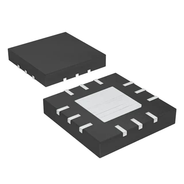
Housed in a 12-lead TQFN with an exposed pad (4 mm × 4 mm body), the MAX5531ETC+ is a surface-mount device. The exposed pad should be soldered to a thermal land on the PCB to improve heat transfer; it also provides a low-impedance ground return.

Linearity and accuracy

The INL is specified at ±4 LSB maximum, and the DNL at ±0.2 LSB maximum. The DNL figure below ±0.5 LSB guarantees monotonicity — the output never decreases for an increasing digital code — which matters in servo loops and programmable power supplies where a non-monotonic step could cause oscillation or a reverse correction.

Lifecycle and compliance

It is ROHS3 compliant, so it meets the European RoHS directive without exemptions.

Frequently asked questions

What is the output type of MAX5531ETC+?

The output type is Voltage - Buffered, meaning the DAC output is driven by an internal buffer amplifier capable of sourcing or sinking current without an external op-amp.

Does MAX5531ETC+ have an internal reference?

Yes, the reference type is Internal, so no external reference IC is needed — the DAC uses its own on-chip reference to set the output full-scale voltage.

Is MAX5531ETC+ lead-free and RoHS compliant?

Yes, it is ROHS3 compliant, meeting the latest RoHS directive without exemptions.