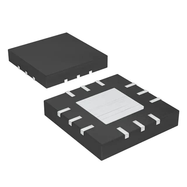
Analog Devices MAX5530ETC+ — Analog & Data Acquisition

MAX5530ETC+ 12-bit DAC, SPI, 660µs settling, 12-TQFN

MPNMAX5530ETC+
End of Life

Analog Devices MAX5530ETC+, 12-bit voltage-output DAC, SPI interface, R-2R architecture, 660µs settling time, single 1.8V-5.5V supply, industrial -40°C to +85°C, 12-TQFN package.

$6.18Ref. price · indicative, final on quote
Packaging12-WQFN Exposed Pad
StockContact for availability
MOQ1 pcs
  • 100% new & originalTraceable channels only — no refurbs, no pulls, no remarked parts.
  • Date & lot codes on quoteStated per line before you commit; label photos on request.
  • MSL-compliant ESD packingMoisture-sealed bags with indicator cards; reels photo-verified.
  • PayPal buyer protectionPay by T/T, PayPal or Payoneer — card payments covered end to end.

Specifications

MAX5530ETC+ Technical Specifications
ParameterValue
Output typeVoltage - Buffered
Mounting typeSurface Mount
Reference typeExternal
Voltage - supply, analog1.8V ~ 5.5V
Voltage - supply, digital1.8V ~ 5.5V
InterfaceSPI
Operating temperature-40°C ~ 85°C
PackageTube
ArchitectureR-2R
INL (DNL)±4, ±0.2
Settling time660µs (Typ)
Number of bits12
Case12-WQFN Exposed Pad
Differential outputNo
Number of d (A converters)1

Product details

What this DAC is and where it fits

The MAX5530ETC+ is a single-channel 12-bit voltage-output DAC from Analog Devices, built around an R-2R ladder architecture. It communicates over an SPI interface and delivers a buffered output that settles within 660 µs typical. The part runs off a single supply from 1.8 V to 5.5 V, with the analog and digital rails sharing the same voltage range, which simplifies power distribution on the board. An external voltage reference sets the output span. The 12-TQFN package (4x4 mm) with exposed pad helps thermal management in tight layouts.

660 µs settling time — what it means for the control loop

The typical settling time is 660 µs.

Package and temperature grade

The MAX5530ETC+ is rated for the industrial temperature range of -40°C to 85°C, which covers most factory-floor, outdoor telecom, and automotive-cabin environments. The 12-TQFN package with exposed pad (4x4 mm) is a surface-mount footprint that requires a thermal via pattern under the pad for adequate heat sinking if the DAC is driving a heavy load or operating near the upper temperature limit. The exposed pad is also the ground connection for the die — a solid solder joint there is mandatory for both thermal and electrical performance.

Sourcing and lifecycle

The part is ROHS3 compliant.

Frequently asked questions

What is the settling time of the MAX5530ETC+?

The typical settling time is 660 µs, which supports update rates around 1.5 kHz for the analog output.

What is the closest pin-compatible alternative to the MAX5530ETC+?

The MAX5530ETC+ is a single-channel device in the MAX5530 family. A pin-compatible alternative within the same family would share the same 12-TQFN footprint and SPI interface. No specific alternate MPN is listed in the available records.