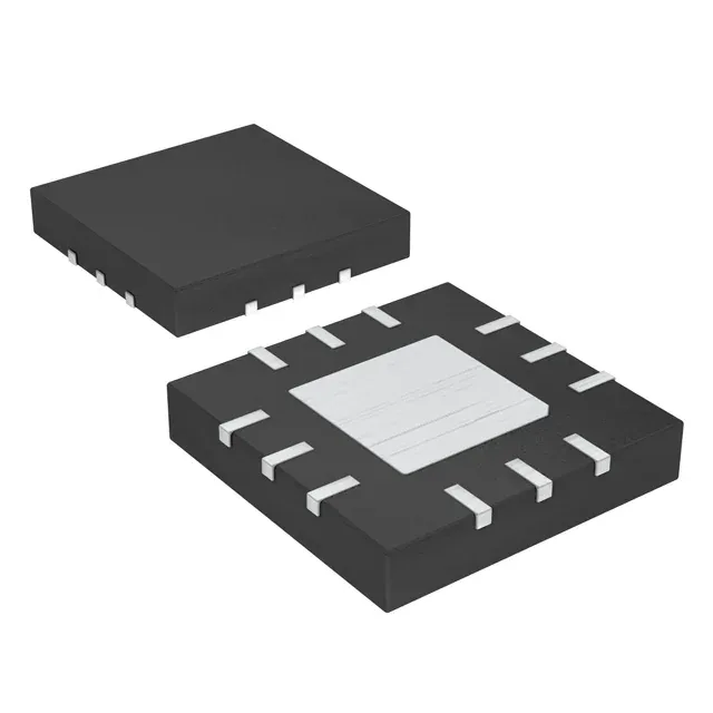
Analog Devices MAX5521ETC+ — Microcontrollers & Processors (MCU / MPU / DSP)

MAX5521ETC+ 10-bit DAC, SPI, Voltage-Out, 12-TQFN

MPNMAX5521ETC+
End of Life

Analog Devices MAX5521ETC+ 10-bit DAC, Voltage - Buffered output, SPI interface, 660 µs settling time, 12-WQFN Exposed Pad, Tube.

$6.78Ref. price · indicative, final on quote
Packaging12-WQFN Exposed Pad
StockContact for availability
Lead timeIn Stock wk
MOQ1 pcs
  • 100% new & originalTraceable channels only — no refurbs, no pulls, no remarked parts.
  • Date & lot codes on quoteStated per line before you commit; label photos on request.
  • MSL-compliant ESD packingMoisture-sealed bags with indicator cards; reels photo-verified.
  • PayPal buyer protectionPay by T/T, PayPal or Payoneer — card payments covered end to end.

Specifications

MAX5521ETC+ Technical Specifications
ParameterValue
Output typeVoltage - Buffered
Mounting typeSurface Mount
Reference typeInternal
Voltage - supply, analog1.8V ~ 5.5V
Voltage - supply, digital1.8V ~ 5.5V
InterfaceSPI
Operating temperature-40°C ~ 85°C
PackageTube
ArchitectureCurrent Source
INL (DNL)±1, ±0.2
Settling time660µs (Typ)
Number of bits10
Case12-WQFN Exposed Pad
Differential outputNo
Number of d (A converters)1

Product details

10-bit DAC with voltage-buffered output

The MAX5521ETC+: The internal reference type means no external reference IC is required; the DAC generates its own full-scale voltage from the supply rails. Architecture is a current-source DAC followed by a voltage buffer — this topology delivers monotonic performance with the ±0.2 LSB DNL figure, which guarantees no missing codes across the full output range.

Settling time and update rate

Typical settling time is 660 µs to 0.5 LSB for a full-scale step — this sets the maximum update rate at roughly 1.5 kHz for a 10-bit output transition. For applications like set-point control in a PID loop or trimming a power supply, this is fast enough for most closed-loop updates. The SPI data interface operates up to the DAC's internal shift-clock limit; the 660 µs settling time, not the SPI clock rate, is the throughput bottleneck.

Housed in a 12-lead WQFN with exposed pad (4x4 mm TQFN footprint per the supplier device package). Tube packaging is standard for this order code; for reel quantities, check the alternate order code suffix at RFQ.

Frequently asked questions

What is the settling time and what does it mean for my update rate?

The typical settling time is 660 µs for a full-scale step. This means the DAC output reaches within 0.5 LSB of the final value in 660 µs, limiting the maximum update rate to roughly 1.5 kHz for a 10-bit transition.