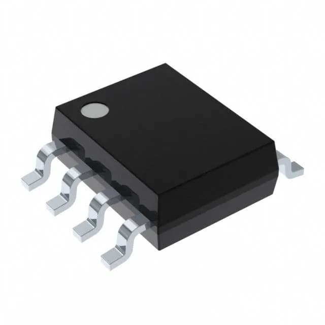
Analog Devices MAX541ACSA+ — Analog & Data Acquisition

MAX541ACSA+ 16-bit DAC, 1µs settling, SPI, 8-SOIC

MPNMAX541ACSA+
End of Life

Maxim Integrated MAX541ACSA+, 16-bit voltage-output DAC, unbuffered R-2R, SPI, 1µs settling, ±0.5 LSB INL/DNL, single 5V supply, 8-SOIC, 0°C to 70°C.

$36.68Ref. price · indicative, final on quote
Packaging8-SOIC (0.154", 3.90mm Width)
StockContact for availability
MOQ1 pcs
  • 100% new & originalTraceable channels only — no refurbs, no pulls, no remarked parts.
  • Date & lot codes on quoteStated per line before you commit; label photos on request.
  • MSL-compliant ESD packingMoisture-sealed bags with indicator cards; reels photo-verified.
  • PayPal buyer protectionPay by T/T, PayPal or Payoneer — card payments covered end to end.

Specifications

MAX541ACSA+ Technical Specifications
ParameterValue
Output typeVoltage - Unbuffered
Mounting typeSurface Mount
Reference typeExternal
Voltage - supply, analog5V
Voltage - supply, digital5V
InterfaceSPI
Operating temperature0°C ~ 70°C
PackageTube
ArchitectureR-2R
INL (DNL)±0.5, ±0.5
Settling time1µs (Typ)
Number of bits16
Case8-SOIC (0.154\", 3.90mm Width)
Differential outputNo
Number of d (A converters)1

Product details

16-bit DAC with 1 µs settling — what it means for the analog output path

The MAX541ACSA+ from Maxim Integrated is a 16-bit, single-channel, voltage-output digital-to-analog converter built around an R-2R ladder architecture. Its unbuffered voltage output and 1 µs typical settling time make it a fit for precision waveform generation, closed-loop setpoint control, and ATE pin electronics where the DAC updates a new value within one microsecond and holds it with 16-bit resolution. The SPI data interface keeps the pin count low — only three wires for the serial clock, data in, and chip select — and the 8-SOIC package fits on compact mixed-signal boards alongside a microcontroller or FPGA.

Single 5 V supply, external reference — power rail simplicity

The MAX541ACSA+ runs on a single 5 V supply for both analog and digital sections. The reference input is external; the user picks the voltage reference that sets the output full-scale range.

Active production — no obsolescence concern

The MAX541ACSA+ is listed as an active product and carries ROHS3 compliance. There is no end-of-life notice or last-time-buy window to track. The 0°C to 70°C temperature grade limits it to commercial/indoor equipment — not rated for automotive or extended industrial ambient.

Frequently asked questions

What is the closest pin-compatible alternative to the MAX541ACSA+?

The MAX542 is a pin-compatible 16-bit DAC in the same family, but the MAX541ACSA+ uses an unbuffered voltage output while the MAX542 includes an internal output buffer. Check the output drive requirement of your load before substituting — the unbuffered output of the MAX541ACSA+ needs an external op-amp for low-impedance loads, whereas the MAX542 drives them directly.

What is the output type and package of the MAX541ACSA+?

The MAX541ACSA+ provides an unbuffered voltage output and is supplied in an 8-SOIC (0.154", 3.90 mm width) surface-mount package. The supplier device package is 8-SOIC.

Does the MAX541ACSA+ have a datasheet PDF?

Yes, a full datasheet PDF for the MAX541ACSA+ is available from Maxim Integrated. The datasheet contains the complete electrical specifications, timing diagrams for the SPI interface, application circuits showing the external reference and output buffer connection, and the package outline drawing for the 8-SOIC footprint.