12-bit voltage-output DAC with SPI — what the ratings mean for your BOM
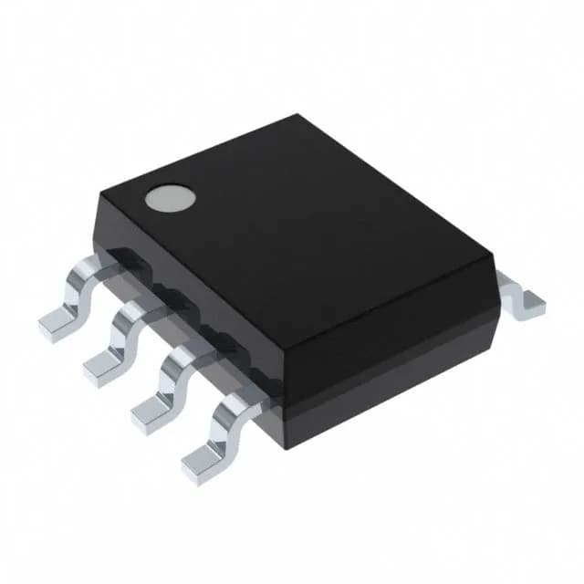
The MAX538BESA+ from Maxim Integrated is a single-channel, 12-bit digital-to-analog converter with a buffered voltage output and an R-2R ladder architecture. It communicates over a standard SPI data interface, making it a straightforward drop-in for any MCU with a spare SPI port. The 25 µs typical settling time means you can update the output at roughly 40 kHz without worrying about the previous value bleeding into the next — fine for set-point control in industrial loops, programmable voltage references, or sensor excitation. The ±1 LSB max INL and DNL guarantees monotonicity across codes, so you won't see non-monotonic glitches in servo or trim applications. Both the analog and digital supply rails run from a single 5 V supply, which keeps the power routing simple and lets you share a common 5 V rail with the rest of the analog front end. The industrial temperature range of -40°C to +85°C covers outdoor telecom cabinets, factory-floor PLCs, and engine-bay control modules without needing a separate temperature grade.
Active lifecycle — no LTB clock ticking
This is a straightforward BOM line — no shortage-driven redesign needed, no broker-only dependency. The part is ROHS3 compliant, which clears the environmental compliance gate for new designs going into EU or California-regulated markets.
Package and footprint — 8-SOIC, tube delivery
The device comes in an 8-pin SOIC package with a 0.154-inch body width and 3.90 mm nominal width, surface-mount. The supplier device package is listed as 8-SOIC. It ships in a Tube, which is typical for small-quantity prototyping and low-volume production runs — if you need tape-and-reel for pick-and-place, check the alternate ordering code (MAX538BESA+T). The standard SOIC-8 footprint is widely supported by assembly houses, and the pin pitch is the standard 1.27 mm.