Dual 12-bit DAC with R-2R architecture
The MAX532BCPE+ is a 12-bit, dual-channel, voltage-buffered DAC from Analog Devices, built on an R-2R ladder architecture. It converts digital SPI data into two independent analog outputs with a typical settling time of 2.5 µs.
Linearity and accuracy
Integral and differential non-linearity are each specified at ±1 LSB maximum. This means every output code lands within one LSB of the ideal transfer function — no missing codes, no systematic bow across the range. For a 12-bit converter with a 4.096 V reference, 1 LSB is 1 mV; the ±1 LSB INL guarantee keeps the total unadjusted error below 2 mV at any code.
Supply rails and reference
Analog supplies span ±11.4 V to ±16.5 V, letting the output swing close to the rails when the reference is set near the positive supply. The reference is external — the output full-scale is set by the voltage applied to the REF pin, not a buried bandgap. This gives the designer control over the span per channel.
This suits controlled indoor environments — bench instrumentation, lab equipment, industrial control cabinets with passive cooling — but not extended or automotive temperature excursions.
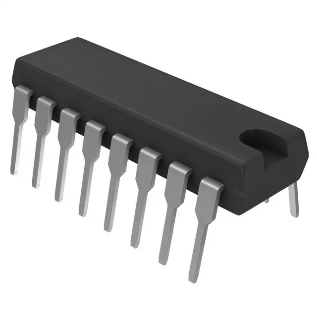
Housed in a 16-pin PDIP (0.300-inch body width, 7.62 mm). Through-hole mounting — the pins are on 100-mil centers and fit standard solder-tail or turned-pin sockets. The wide body leaves room for routing traces between pads on a two-layer board.