Active lifecycle — sourcing reality
The MAX5156BCEE+: No stock-holding claim is made here.
12-bit dual DAC with SPI interface
This is a 12-bit, dual-channel, voltage-buffered DAC built on an R-2R architecture. The two converters are independently addressed via the SPI data interface, allowing simultaneous or sequential updates from a single digital bus. Typical settling time is 15 µs to ±0.5 LSB, which sets the per-channel update rate ceiling — useful for closed-loop control loops or trim adjustments that must settle before the next sample window closes. Both analog and digital supply rails are specified at 5 V, simplifying the power tree to a single regulated rail. The external reference input allows the output span to be scaled independently of the supply.
Linearity and precision for the BOM
INL and DNL are both specified at ±1 LSB maximum — no missing codes guaranteed over the operating range. This is the key linearity spec for a 12-bit system: a ±1 LSB INL means the transfer function stays within one-quarter of a 12-bit step at the worst point, which is adequate for most industrial set-point and calibration DAC applications. The commercial temperature grade (0°C to 70°C) covers indoor equipment, bench instrumentation, and telecom central-office environments. For extended-temperature or automotive use, a different grade would be needed.
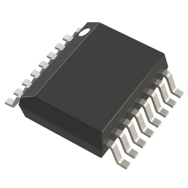
The supplier device package is 16-QSOP, which is the Analog Devices designation for this form factor. Surface-mount assembly, shipped in tube format. The package is compatible with standard reflow profiles for mixed-signal boards. No exposed thermal pad — thermal dissipation is through the leads and board copper.
Compliance and documentation
ROHS3 compliant. Analog Devices provides the full datasheet and application notes for this part — the SPI timing diagram, reference input range, and output drive capability are detailed in the official documentation.