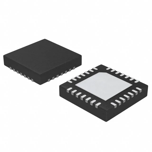
Buck controller in a 5x5 QFN — what the package and pinout mean for the board
The MAX5060ATI+ is a step-down (buck) switching controller in a 28-WFQFN exposed-pad package, supplier device package 28-TQFN (5x5). The QFN footprint is reworkable with hot air if the stencil aperture for the thermal pad is split into four quadrants — a single large opening wicks too much solder and lifts the part off the board. Pin 1 is marked by a chamfer on the package corner; the exposed pad is the ground connection, so the solder joint under the part must be void-free to keep the thermal resistance low.
Switching frequency range and clock sync — placing the noise where you want it
The clock sync input lets the controller lock to an external clock within that band — useful when the switcher's fundamental must sit between two sensitive frequency bins in a radio or sensor front-end. At 1.5 MHz the inductor shrinks to a 2.2 µH or 3.3 µH footprint, but the switching losses in the external FETs rise. The 125 kHz end trades inductor size for efficiency — a 10 µH or 15 µH coil keeps the ripple current low at the cost of board area. The controller itself does not dissipate much; the external FETs and inductor set the thermal budget.
Supply range and control hooks — fitting into a 24 V industrial bus
The Vcc supply range is 4.75 V to 28 V, which covers 5 V and 12 V rails with headroom for transients. On a 24 V industrial bus the part runs without an external pre-regulator — the 28 V max gives margin for the typical 30 V surge on a 24 V line. The undervoltage lockout threshold is set internally; the enable pin provides an external on/off control for sequencing. Control features include current limit (cycle-by-cycle on the external FET), frequency control (the RT pin), and a power-good output that flags when the output is within regulation. These hooks are enough to sequence multiple rails without a separate supervisor — the power-good from one MAX5060 can enable the next converter in the chain.
Active production — sourcing posture for this buck controller
The 28-TQFN (5x5) package is a standard Analog Devices footprint; if a second source is needed, the board layout must accommodate a different pinout.