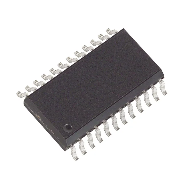
10-bit DAC with R-2R core and voltage-buffered output
The MAX503CWG+T is a single-channel 10-bit digital-to-analog converter from Analog Devices, built on an R-2R ladder architecture with an internal output buffer. It delivers a voltage output that can directly drive an ADC input or analog control node without an external op-amp stage. Resolution is 10 bits — 1024 distinct output levels — with integral nonlinearity (INL) held to ±0.5 LSB maximum and differential nonlinearity (DNL) within ±1 LSB maximum. The R-2R topology guarantees monotonicity across the full code range, so no missing codes occur at the 10-bit level.
Settling time and interface — what limits the update rate
Output settling time is 25 µs typical to ±0.5 LSB for a full-scale step. This sets the maximum update rate at roughly 40 kHz for full-swing transitions, though smaller code steps settle faster. For a control loop updating at 10 kHz, the DAC has adequate margin. The data interface is parallel — all 10 bits are latched simultaneously on a single write strobe. No serial clock overhead, so the bus write time is one memory-cycle wide, suitable for DSP or microcontroller parallel ports.
Supply rails and reference options
Analog supply is ±5 V, digital supply is 5 V — these are the only rails required. The reference can be either external (applied to the REF pin) or internal (the on-chip bandgap). Using the internal reference simplifies the BOM by one reference IC but ties the full-scale voltage to the bandgap tolerance; an external reference lets the user set the output span to match the ADC's input range.
Package and assembly — 24-SOIC wide-body
The wide-body SOIC footprint is standard for reflow assembly; the reel format suits automated pick-and-place for volume production. Mounting is surface-mount only. The 24-SOIC body width requires a pad pattern matching the 7.50 mm package — verify the board layout accepts this footprint before specifying.
Production status is Active — the MAX503CWG+T is in current manufacture with no announced end-of-life. ROHS3 compliant (no exemptions).