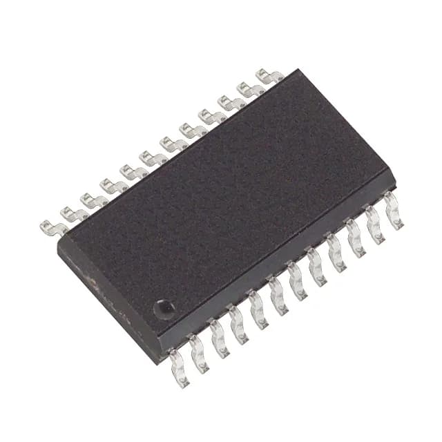
Analog Devices MAX503CWG+ — Memory (DRAM / SRAM / Flash / EEPROM)

MAX503CWG+ 10-Bit Voltage-Output DAC, 25µs Settling, 24-SOIC

MPNMAX503CWG+
End of Life

Maxim MAX503CWG+ 10-bit voltage-output DAC, R-2R architecture, 25µs settling, parallel interface, ±5V analog / 5V digital supply, 0°C to 70°C, 24-SOIC package.

$7.45Ref. price · indicative, final on quote
Packaging24-SOIC (0.295", 7.50mm Width)
StockContact for availability
MOQ1 pcs
  • 100% new & originalTraceable channels only — no refurbs, no pulls, no remarked parts.
  • Date & lot codes on quoteStated per line before you commit; label photos on request.
  • MSL-compliant ESD packingMoisture-sealed bags with indicator cards; reels photo-verified.
  • PayPal buyer protectionPay by T/T, PayPal or Payoneer — card payments covered end to end.

Specifications

MAX503CWG+ Technical Specifications
ParameterValue
Output typeVoltage - Buffered
Mounting typeSurface Mount
Reference typeExternal, Internal
Voltage - supply, analog±5V
Voltage - supply, digital5V
InterfaceParallel
Operating temperature0°C ~ 70°C
PackageTube
ArchitectureR-2R
INL (DNL)±0.5 (Max), ±1 (Max)
Settling time25µs (Typ)
Number of bits10
Case24-SOIC (0.295\", 7.50mm Width)
Differential outputNo
Number of d (A converters)1

Product details

What this DAC is and where it fits

The Maxim MAX503CWG+ is a 10-bit digital-to-analog converter with a buffered voltage output and an R-2R ladder architecture. It takes a parallel digital word and converts it to an analog voltage, settling to within 1 LSB in 25 µs typical — fast enough for process-control setpoints, motor-drive reference ramps, or ATE forcing functions that update in the tens of kilohertz range. The single DAC channel uses an external or internal reference, and the output is rail-to-rail capable on a ±5 V analog supply with a separate 5 V digital supply.

Key ratings and what they mean for your BOM

The 25 µs settling time sets the maximum update rate: you can drive a new output value every 25 µs. The ±0.5 LSB max INL and ±1 LSB max DNL mean the transfer curve stays monotonic and linear to within half a least-significant bit.

Lifecycle and sourcing

This part carries an Active lifecycle status and is ROHS3 compliant. No last-time-buy or end-of-life notice is on record.

Package and handling

The MAX503CWG+ comes in a 24-pin SOIC wide-body (7.50 mm width) and ships in a tube. Surface-mount, so it needs a reflow profile — not a field-swap candidate without a hot-air station. The wide-body SOIC is easier to hand-solder than the narrow version, but still requires a steady hand and a fine tip. Orientation is marked by pin 1 dimple on the package top; the tube keeps the parts aligned for pick-and-place. No ESD-sensitive handling beyond standard CMOS precautions.

Frequently asked questions

What is the settling time of MAX503CWG+?

The typical settling time is 25 µs to within 1 LSB for a full-scale step. That sets the maximum update rate at roughly 40 kHz.

What is the data interface of MAX503CWG+?

It uses a parallel digital interface — 10 data lines plus control signals. No serial clock or protocol overhead, but it ties up more GPIO pins than a SPI or I²C DAC.