What the 4-ohm on-resistance means for your signal chain
The MAX4652ESE+ is a quad SPST-NO analog switch from Analog Devices, built for precision signal routing where the switch's own resistance must not dominate the measurement. Each channel presents a maximum 4-ohm on-resistance, with channel-to-channel matching held to 50 milliohms — this matching matters when you are switching gain-setting resistors in a programmable amplifier or routing a reference voltage across multiple ADC inputs, because the offset error between channels stays within a tight band. The 1:1 multiplexer/demultiplexer topology with normally-open contacts means each switch is a single-pole single-throw that closes on command — no break-before-make logic to sequence, just a clean connect or disconnect per channel.
Switching speed and signal integrity for fast multiplexing
Turn-on time is 14 ns maximum, turn-off time 8 ns maximum — the asymmetry is typical of CMOS switches where the turn-off path discharges the gate faster than the turn-on path charges it. For a multiplexer scanning four channels at 10 MHz, the 14 ns settling window sets the minimum sample period before the downstream ADC can take a valid reading. Crosstalk is rated at -100 dB at 1 MHz, which means less than 10 ppm of a 1 MHz signal on one channel couples into an adjacent off-channel. For a 16-bit ADC with 96 dB SNR, this crosstalk floor sits below the converter's own noise — the switch does not become the limiting factor in the isolation budget. Charge injection is 2 pC typical — the charge dumped onto the signal line when the switch opens or closes. In a sample-and-hold front end, 2 pC into a 10 pF hold capacitor produces a 200 mV glitch; the designer must budget this into the acquisition time or add a track-and-hold ahead of the switch.
Leakage, capacitance, and the supply rail envelope
Off-channel leakage current is 100 pA maximum — at 25°C this is negligible for a 10-kiloohm source impedance (1 µV error), but the leakage doubles roughly every 10°C. At 85°C the leakage approaches 1.6 nA, which on a 1-megaohm source produces 1.6 mV of offset — worth checking if the signal source is high-impedance. Channel capacitance is 16 pF on both the source and drain sides. This capacitance, combined with the 4-ohm on-resistance, forms an RC low-pass filter with a -3 dB corner around 2.5 GHz — well above any practical analog bandwidth, so the switch does not roll off the signal in the audio or low-MHz range. The temperature grade is industrial: -40°C to +85°C, covering factory-floor and outdoor telecom enclosures.
Package, compliance, and production status
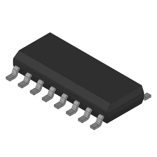
The standard SOIC footprint is widely supported in PCB layout libraries and reflow profiles. It ships in a tube, which is the typical handling format for low-volume production or prototyping — not tape-and-reel, so plan for manual placement or a tube feeder if running automated assembly.